MT48LC64M8A2TG-75 L:C TR
| Part Description |
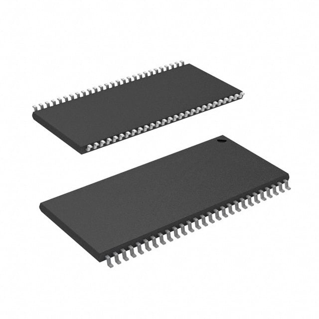
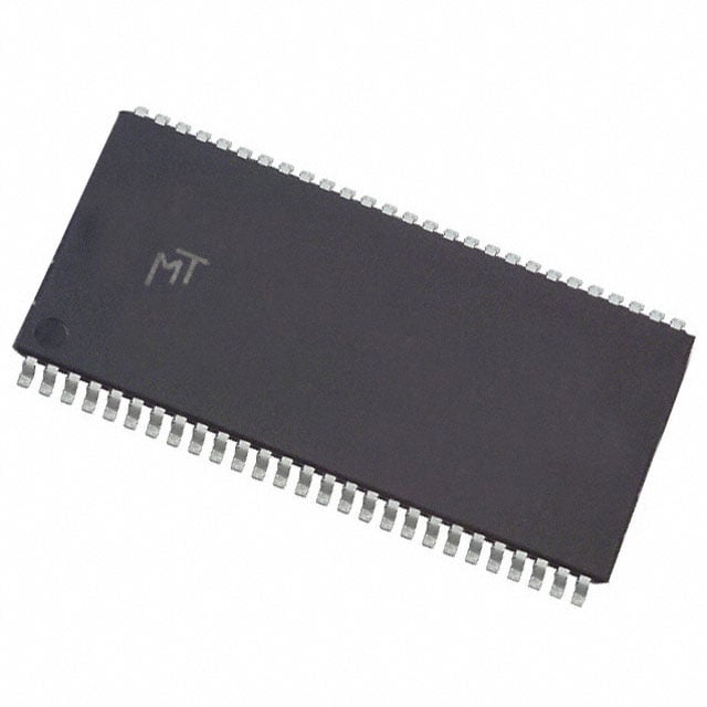
IC DRAM 512MBIT PAR 54TSOP II |
|---|---|
| Quantity | 198 Available (as of June 15, 2026) |

| Product Category | DRAM Memory |
|---|---|
| Manufacturer | Micron Technology Inc. |
| Manufacturing Status | Obsolete |
| Manufacturer Standard Lead Time | Contact Us |
| Datasheet |
Specifications & Environmental
| Device Package | 54-TSOP II | Memory Format | DRAM | Technology | SDRAM | ||
|---|---|---|---|---|---|---|---|
| Memory Size | 512 Mbit | Access Time | 5.4 ns | Grade | Commercial | ||
| Clock Frequency | 133 MHz | Voltage | 3V ~ 3.6V | Memory Type | Volatile | ||
| Operating Temperature | 0°C ~ 70°C (TA) | Write Cycle Time Word Page | 15 ns | Packaging | 54-TSOP (0.400", 10.16mm Width) | ||
| Mounting Method | Volatile | Memory Interface | Parallel | Memory Organization | 64M x 8 | ||
| Moisture Sensitivity Level | 4 (72 Hours) | RoHS Compliance | RoHS non-compliant | REACH Compliance | REACH Unaffected | ||
| Qualification | N/A | ECCN | EAR99 | HTS Code | 8542.32.0024 |
Overview of MT48LC64M8A2TG-75 L:C TR – IC DRAM 512MBIT PAR 54TSOP II
The MT48LC64M8A2TG-75 L:C TR is a 512 Mbit SDR SDRAM organized as 64M × 8 with four internal banks and a parallel memory interface. It is a fully synchronous DRAM device with on-chip features for pipelined operation and programmable burst lengths.
Designed for systems requiring PC100- and PC133-compliant synchronous DRAM, this device delivers board-level, 3.3 V single-supply memory in a compact 54-pin TSOP II (400 mil / 10.16 mm) package and operates over a commercial temperature range of 0 °C to +70 °C.
Key Features
- Core / Architecture SDR SDRAM; fully synchronous with all signals registered on the positive edge of the system clock and internal pipelined operation for column-address changes every clock cycle.
- Memory Organization 512 Mbit density arranged as 64M × 8 with four internal banks.
- Standards Compliance PC100- and PC133-compliant timing options as specified in the device datasheet.
- Timing and Performance Clock frequency up to 133 MHz (speed grade -75) with an access time of 5.4 ns (documented for CL = 3 at 133 MHz); programmable CAS latencies and burst lengths (1, 2, 4, 8, or full page).
- Refresh and Power Management Supports auto refresh, self refresh, concurrent auto precharge and auto refresh modes, and a 64 ms, 8192-cycle refresh specification.
- Power Supply Single-supply operation at 3.3 V (specified range 3.0 V to 3.6 V).
- Package and Temperature 54-pin TSOP II (400 mil, 10.16 mm width) plastic package; commercial operating temperature range 0 °C to +70 °C.
- I/O Compatibility LVTTL-compatible inputs and outputs as documented in the datasheet.
Typical Applications
- PC100 / PC133-compliant systems — Provides standard-compliant synchronous DRAM timing and densities for systems requiring PC100 or PC133 memory.
- Board-level memory expansion — Compact 54-pin TSOP II package for designs with constrained PCB space that require 512 Mbit SDRAM.
- 3.3 V single-supply designs — Direct support for systems operating from a 3.3 V ±0.3 V supply.
- Parallel SDRAM interfaces — Suited to designs using a parallel SDRAM architecture with programmable burst and auto-precharge features.
Unique Advantages
- Standards compliance: PC100- and PC133-compliant timing options simplify integration into systems expecting these SDRAM timing profiles.
- Flexible burst and bank management: Programmable burst lengths and internal bank architecture enable efficient, pipelined data transfers and improved throughput within the device’s specified timing.
- Compact package: 54-pin TSOP II (400 mil) package offers a board-friendly form factor for 512 Mbit SDRAM integration where space is limited.
- Robust refresh and low-power modes: Auto refresh and self-refresh support with an 8K refresh count (64 ms, 8192-cycle) provide reliable data retention and power management options.
- Industry-standard voltage: Single 3.3 V supply operation (3.0 V–3.6 V) aligns with common system power rails for straightforward power design.
Why Choose MT48LC64M8A2TG-75 L:C TR?
The MT48LC64M8A2TG-75 L:C TR delivers a 512 Mbit SDR SDRAM solution with PC100/PC133-compliant timing, a 64M × 8 organization, and a compact 54-pin TSOP II package. Its fully synchronous design, programmable burst options, and internal bank architecture provide predictable timing and flexible data transfer modes for systems that require standard SDRAM behavior.
This device is suitable for engineers and procurement teams seeking a documented, single-supply 3.3 V SDRAM component for designs operating over the commercial temperature range. The combination of industry-standard timing, refresh capabilities, and a space-efficient package supports reliable, board-level memory integration.
Request a quote or submit a sales inquiry to evaluate the MT48LC64M8A2TG-75 L:C TR for your next design requirement.