
A31G336CL
| Part Description |
A31G336 32-bit ARM Cortex-M0+ Microcontroller |
|---|---|
| Quantity | 1,916 Available (as of October 16, 2026) |

| Product Category | Microcontrollers |
|---|---|
| Manufacturer | ABOV Semiconductor |
| Manufacturing Status | Mass Production |
| Manufacturer Standard Lead Time | Contact Us |
| Datasheet |
Specifications & Environmental
| Connectivity | I2C, SPI, UART/USART, USB | Core Processor | ARM Cortex-M0+ | Core Size | 32-Bit | ||
|---|---|---|---|---|---|---|---|
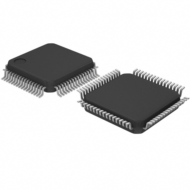
| Data Converters | A/D 10x12b | Device Package | 48-LQFP | ECCN | 3A991.a.2 | ||
| EEPROM Size | 0 Kbytes | HTS Code | 8542.31.00.00 | Moisture Sensitivity Level | N/A | ||
| Mounting Method | Surface Mount | Number of I/O | 37 | Operating Temperature | -40°C - 85°C | ||
| Oscillator Type | Internal/External | Package / Case | 48-LQFP (7x7mm) | Program Memory Size | 256 Kbytes | ||
| Program Memory Type | FLASH | RAM Size | 32 Kbytes | REACH Compliance | Unknown | ||
| RoHS Compliance | Unknown | Speed | 48 MHz | Voltage | 1.8V - 5.5V |
Overview of A31G336CL – A31G336 32-bit ARM Cortex-M0+ Microcontroller
The A31G336CL is a 32-bit microcontroller based on the energy-efficient ARM Cortex-M0+ core, designed for embedded control applications that require a compact footprint and integrated peripheral set. It combines up to 256 KB of code flash (with ECC and read protection) and 32 KB of SRAM with a rich mix of analog, timing and communication peripherals.
Operating from 1.8 V to 5.5 V and running up to 48 MHz, the A31G336CL targets embedded systems that need deterministic control, sensor interfacing and USB connectivity while offering flexible power modes and a robust set of system reliability features.
Key Features
- Core Arm Cortex-M0+ 32‑bit core supporting operation up to 48 MHz for efficient embedded control and processing.
- Memory 256 KB code Flash with ECC and read protection, plus 32 KB on-chip SRAM for program and data storage.
- Power and Clock Wide operating voltage range 1.8–5.5 V; RUN, SLEEP and DEEP‑SLEEP modes; internal RC and external oscillator options; clock monitoring and power management functions; Low Voltage Detection/Reset (LVI/LVR) and POR.
- Timers and PWM Multiple timer resources including six 16‑bit timer channels and two 32‑bit timers supporting timer/counter, one‑shot, PWM and capture modes with a 12‑bit prescaler.
- Analog and Sensing 12‑bit A/D converter with 10 analog input channels (A31G336CL) and up to 1 Msps conversion rate, plus two on‑chip comparators for analog monitoring.
- Connectivity USB 2.0 Full Speed with crystal‑less clock management and on‑chip packet buffer SRAM; multiple serial interfaces including four USART ports, three I2C ports and two SPI ports.
- DMA and Peripheral Integration Four‑channel DMA supporting 8/16/32‑bit transfers across internal peripherals to reduce CPU load and accelerate data movement.
- System Reliability CRC calculation unit (multiple CRC modes), 24‑bit watchdog timer with reset/interrupt options, nested vectored interrupt controller (NVIC) with 31 interrupt sources, and flash read protection.
- Real‑Time and Debug Real Time Timer and Calendar (RTCC) for timekeeping and scheduling, and Serial Wire Debug (SWD) interface for development and debug.
- GPIO and Package 37 I/O pins in a 48‑pin LQFP surface‑mount package (7×7 mm, 0.5 mm pitch); rated for operation from −40 °C to 85 °C.
Typical Applications
- Embedded control and automation — Use the Cortex‑M0+ core, multiple timers and NVIC for deterministic control tasks, motor timing and event scheduling.
- Sensor interfacing and data acquisition — On‑chip 12‑bit ADC, comparators and DMA simplify analog signal capture and reduce CPU overhead for sensor hubs and monitoring nodes.
- USB‑enabled devices and peripherals — Built‑in USB Full Speed with crystal‑less operation and packet buffer SRAM supports USB connectivity in compact designs.
- Portable and battery‑powered equipment — Wide 1.8–5.5 V supply range plus sleep and deep‑sleep low power modes enable flexible power architectures and single‑cell operation scenarios.
Unique Advantages
- Energy‑efficient 32‑bit processing: Cortex‑M0+ core delivers 32‑bit performance at low power and supports control workloads up to 48 MHz.
- High on‑chip integration: Flash with ECC, SRAM, ADC, comparators, USB, multiple serial interfaces and DMA reduce external components and simplify BOM.
- Flexible power and clocking: 1.8–5.5 V operation, internal/external oscillators and multiple power modes allow design flexibility across supply schemes.
- Built for reliable operation: Flash read protection, CRC unit, watchdog timer, LVI/LVR and POR provide layers of system integrity and safety features.
- USB capability without crystal: Crystal‑less USB Full Speed with on‑chip packet buffer SRAM enables compact USB‑connected products with fewer external components.
- Compact commercial packaging: 48‑pin LQFP (7×7 mm) surface‑mount package and −40 °C to 85 °C rating support space‑constrained designs and broad environmental use.
Why Choose A31G336CL?
The A31G336CL pairs an energy‑efficient ARM Cortex‑M0+ core with a comprehensive set of on‑chip peripherals—memory with ECC, ADC, multiple timers, USB Full Speed, DMA and serial interfaces—making it a balanced choice for embedded control, sensor interfacing and USB‑enabled applications. Its wide supply range and low‑power modes provide flexible deployment across battery and system‑powered designs.
Delivered in a compact 48‑pin LQFP package and backed by ABOV Semiconductor’s A31G336 family documentation, the A31G336CL offers a robust, well‑specified foundation for designs that need integrated functionality, system reliability and a small footprint.
Request a quote or contact sales to discuss part availability, pricing and how the A31G336CL can meet your design requirements.














Date Founded: 2006
Headquarters: Cheongju-si, Chungcheongbuk-do, Republic of Korea
Employees: 200+
Revenue: $95.4 Million
Certifications and Memberships: ISO9001:2015, ISO14001:2015, UL60730


