
A31G346RL
| Part Description |
A31G346 32-bit Arm Cortex-M0+ Microcontroller |
|---|---|
| Quantity | 1,767 Available (as of October 16, 2026) |

| Product Category | Microcontrollers |
|---|---|
| Manufacturer | ABOV Semiconductor |
| Manufacturing Status | Mass Production |
| Manufacturer Standard Lead Time | Contact Us |
| Datasheet |
Specifications & Environmental
| Connectivity | I2C, SPI, UART/USART | Core Processor | ARM Cortex-M0+ | Core Size | 32-Bit | ||
|---|---|---|---|---|---|---|---|
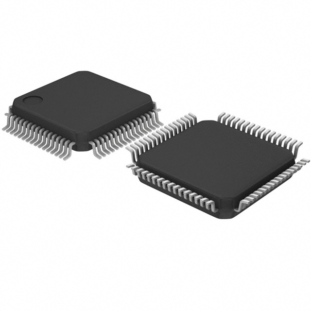
| Data Converters | A/D 10x12b | Device Package | 64-LQFP | ECCN | 3A991.a.2 | ||
| EEPROM Size | 0 Kbytes | HTS Code | 8542.31.00.00 | Moisture Sensitivity Level | N/A | ||
| Mounting Method | Surface Mount | Number of I/O | 50 | Operating Temperature | -40°C - 85°C | ||
| Oscillator Type | Internal/External | Package / Case | 64-LQFP (10x10mm) | Program Memory Size | 256 Kbytes | ||
| Program Memory Type | FLASH | RAM Size | 32 Kbytes | REACH Compliance | Unknown | ||
| RoHS Compliance | Unknown | Speed | 48 MHz | Voltage | 1.8V - 5.5V |
Overview of A31G346RL – A31G346 32-bit Arm Cortex-M0+ Microcontroller
The A31G346 is a general-purpose 32-bit microcontroller built around the energy-efficient Arm Cortex-M0+ core, running up to 48 MHz. It combines up to 256 Kbytes of code Flash and 32 Kbytes of SRAM with a broad set of on-chip peripherals and power management features.
Designed for low-power embedded applications, the A31G346 integrates analog, timer and serial communication resources with power control (POR, LVR/LVI, internal RC oscillator and SLEEP/DEEP‑SLEEP modes) to support compact, power-aware system designs.
Key Features
- Core Arm Cortex-M0+ 32-bit core with up to 48 MHz operation for efficient control and deterministic interrupt handling.
- Memory 256 Kbytes of on-chip Flash (code memory) with read protection and 32 Kbytes of SRAM for application and data storage.
- Voltage and Power Management Wide operating voltage range from 1.8 V to 5.5 V, with POR, Low Voltage Reset (LVR), Low Voltage Indicator (LVI), internal RC oscillator, and RUN/SLEEP/DEEP‑SLEEP modes for power optimization.
- Timers and Real-Time Two 32-bit timers and six 16-bit timers with PWM, capture and one-shot modes plus a Real Time Clock and Calendar (RTCC) for scheduling and timekeeping.
- Analog 12-bit A/D converter with 10 analog input channels and up to 1 Msps conversion rate for data acquisition.
- Communication Interfaces Multiple serial interfaces: four USART ports, three I2C ports and two SPI ports to support diverse peripheral connectivity.
- DMA and CRC Four-channel DMA controller supporting 8/16/32-bit transfers across 19 internal peripherals, plus a CRC calculation unit (CRC‑CCITT, CRC‑16 and user-defined modes) for data integrity.
- System Reliability and Debug Nested Vectored Interrupt Controller (NVIC) with 29 interrupt sources, 24-bit watchdog timer, read protection and Serial Wire Debug (SWD) interface.
- GPIO and I/O Up to 50 I/O pins with external interrupt mapping for flexible system interfacing.
- Package and Temperature Surface-mount 64-LQFP package (10 × 10 mm, 0.50 mm pitch) and commercial operating temperature range of −40 °C to 85 °C.
Typical Applications
- Low-power embedded systems — SLEEP and DEEP‑SLEEP modes, wide VCC range and internal RC oscillator enable energy-aware device designs.
- Sensor data acquisition — 12-bit ADC (10 channels) and DMA support high-rate sampling and efficient data transfer for measurement tasks.
- Real-time control and timing — Multiple timers, RTCC and deterministic NVIC-based interrupt handling for control loops and scheduling.
- Peripheral hubs and interface controllers — Multiple USART, I2C and SPI ports allow aggregation and control of serial peripherals and subsystems.
Unique Advantages
- Highly integrated analog and digital peripherals: On-chip ADC, timers, communication ports, DMA and CRC reduce external component count and simplify BOMs.
- Flexible power envelope: 1.8–5.5 V operation plus multiple low-voltage and reset features enable robust operation across supply conditions.
- Efficient data handling: Four DMA channels working with 19 peripherals accelerate data movement while minimizing CPU load.
- Security and reliability features: Flash read protection, watchdog timer and CRC unit support system integrity and fault recovery strategies.
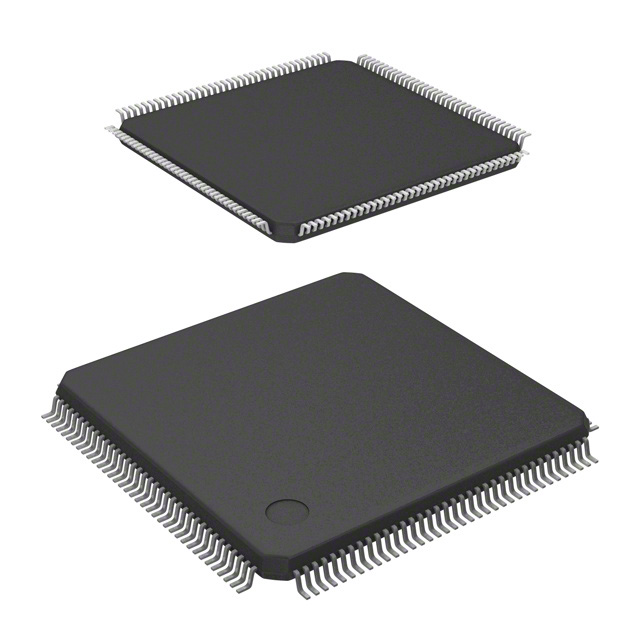
- Compact SMD packaging: 64‑LQFP package provides 50 GPIOs and ample peripheral connectivity in a standard surface-mount footprint.
Why Choose A31G346RL?
The A31G346RL positions itself as a versatile, general-purpose microcontroller that balances processing capability with a wide feature set and power management. With a Cortex‑M0+ core at up to 48 MHz, 256 KB Flash, 32 KB SRAM and integrated ADCs, timers, communications and DMA, it is suited to embedded designs that require measurable performance, peripheral integration and power-aware operation.
This device is well suited for developers and engineers building compact, connected embedded systems that need reliable timing, data acquisition and serial connectivity within a commercial temperature range. The on-chip reliability and debugging features support scalable designs and streamlined development cycles.
Request a quote or submit a product inquiry to receive pricing and lead-time information for the A31G346RL.














Date Founded: 2006
Headquarters: Cheongju-si, Chungcheongbuk-do, Republic of Korea
Employees: 200+
Revenue: $95.4 Million
Certifications and Memberships: ISO9001:2015, ISO14001:2015, UL60730


