
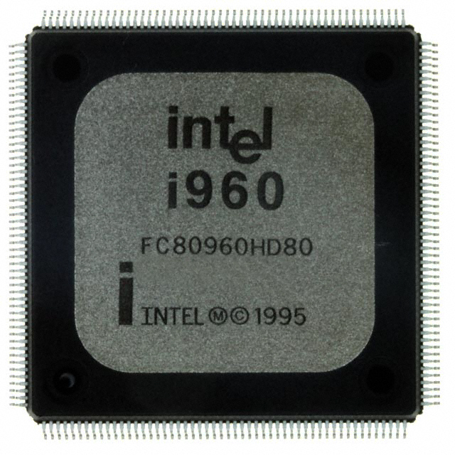
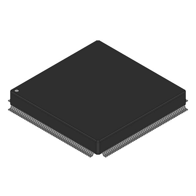
FC80960HD80SL2LZ
| Part Description |
i960 Microprocessor IC i960 1 Core, 32-Bit 80MHz 208-PQFP |
|---|---|
| Quantity | 10 Available (as of October 8, 2026) |
| Product Category | Microprocessors |
|---|---|
| Part Series | i960 Hx |
| Manufacturer | Intel |
| Manufacturing Status | Obsolete |
| Manufacturer Standard Lead Time | Contact Us |
| Datasheet |
Specifications & Environmental
| Core Processor | i960 | Device Package | 208-PQFP | ECCN | 3A001A3 | ||
|---|---|---|---|---|---|---|---|
| Grade | Commercial | Graphics Acceleration | No | HTS Code | 8542.31.0001 | ||
| Moisture Sensitivity Level | 5 (48 Hours) | Mounting Method | Surface Mount | Mounting Type | Surface Mount | ||
| Number of Cores/Bus Width | 1 Core, 32-Bit | Operating Temperature | 0°C ~ 85°C (TC) | Package / Case | 208-QFP | ||
| RAM Controllers | DRAM | REACH Compliance | REACH Unknown | RoHS Compliance | RoHS non-compliant | ||
| Speed | 80MHz | Supplier Device Package | 208-PQFP | Voltage – I/O | 3.3V |
Overview of FC80960HD80SL2LZ – IC MPU I960 80MHZ 208QFP
The FC80960HD80SL2LZ is a single-core, 32-bit i960 microprocessor supplied in a 208-pin PQFP surface-mount package. It runs at an 80 MHz core clock and is supplied with 3.3 V I/O, making it suitable for commercial embedded designs.
Built on the i960 Hx family architecture, this device integrates on-chip floating point support, multi-level caches and system peripherals to deliver high instruction throughput and integrated system functionality for embedded applications.
Key Features
- Core & Performance 32-bit i960 core operating at 80 MHz; capable of issuing up to 150 million instructions per second as specified for the family.
- On-chip FPU Integrated floating-point unit provides hardware acceleration for numeric and signal processing tasks.
- Memory & Cache High-performance on-chip storage including a 16 Kbyte four-way set-associative instruction cache, an 8 Kbyte four-way set-associative data cache and 2 Kbyte general-purpose RAM to reduce external memory traffic.
- Internal Bandwidth 1.28 Gbyte internal bandwidth at 80 MHz and separate 128-bit internal paths for instructions and data for parallel data/instruction flows.
- Bus & External Memory Support 32-bit demultiplexed burst bus with per-byte parity generation/checking, support for 8/16/32-bit external bus widths, address pipelining option and a programmable wait-state generator; external bandwidth quoted at 160 Mbyte/s (40 MHz bus example).
- Interrupts & Timers High-speed interrupt controller supporting up to 240 external interrupts with 31 programmable priorities and dual on-chip 32-bit timers with auto-reload and one-shot modes.
- System Protection & Debug Guarded Memory Unit for user/supervisor read/write/execute protection and JTAG IEEE 1149.1 support for test and debug.
- Power, Package & Temperature 3.3 V I/O (5 V tolerant inputs, TTL-compatible outputs), commercial operating temperature range 0 °C to 85 °C, supplied in a 208-PQFP surface-mount package.
Typical Applications
- Real-time embedded control — Suited for embedded controllers that require deterministic instruction throughput, high interrupt capacity and on-chip timers for scheduling and control loops.
- Communication and I/O subsystems — On-chip bus features, parity protection and significant external bandwidth support system designs that handle sustained data movement and I/O transactions.
- System management and instrumentation — Integrated caches, general-purpose RAM and JTAG debug support simplify development and improve system responsiveness for instrumentation tasks.
Unique Advantages
- Highly integrated processing core: Integrated FPU, caches and general-purpose RAM reduce external component count and simplify board design.
- High internal throughput: 1.28 Gbyte internal bandwidth at 80 MHz and separate instruction/data paths enable parallelism and efficient instruction execution.
- Robust interrupt and timing support: Up to 240 external interrupts and dual 32-bit timers provide fine-grained control for real-time embedded applications.
- Flexible external memory interface: Demultiplexed burst bus with per-byte parity and programmable wait states supports a range of external memory configurations and reliability options.
- Built-in system protection and testability: Guarded Memory Unit for privilege-based memory protection plus IEEE 1149.1 JTAG support for production test and debugging.
- Standard commercial compatibility: 3.3 V I/O with 5 V tolerant inputs and a commercial temperature grade (0 °C to 85 °C) for general embedded deployments.
Why Choose FC80960HD80SL2LZ?
The FC80960HD80SL2LZ delivers a balanced combination of 32-bit processing performance, on-chip floating-point acceleration and integrated system features that simplify embedded system design. Its multi-level caches, internal RAM and high internal bandwidth are designed to improve instruction throughput while reducing external memory dependency.
This part is well suited to designers seeking a commercially graded, surface-mount i960 processor with comprehensive interrupt, timer and bus features for embedded control, communication or instrumentation systems. The integrated protection and JTAG support provide added reliability and testability for production deployments.
Request a quote or submit an inquiry for pricing and availability of FC80960HD80SL2LZ to move your design forward.





















Date Founded: 1968
Headquarters: Santa Clara, California, USA
Employees: 130,000+
Revenue: $54.23 Billion
Certifications and Memberships: ISO9001:2015, ISO14001:2015, ISO17025:2017, ISO27001:2022, ISO45001:2018, ISO50001:2018


