
KMPC875VR133
| Part Description |
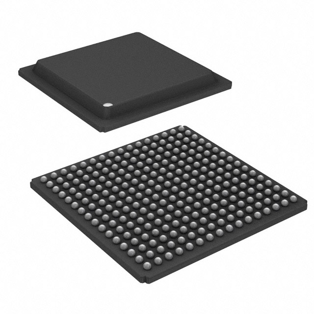
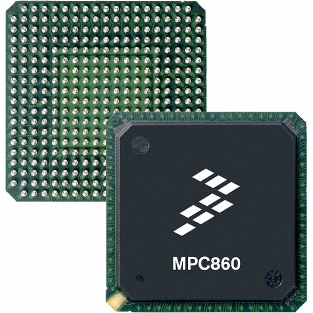
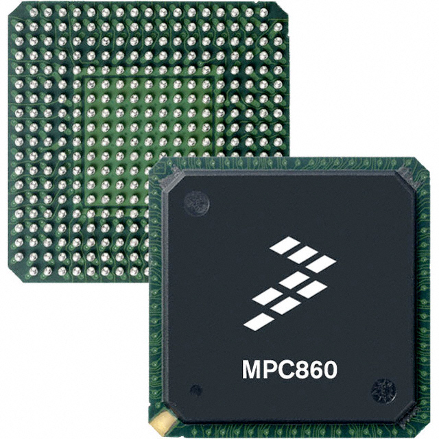
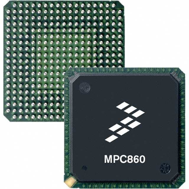
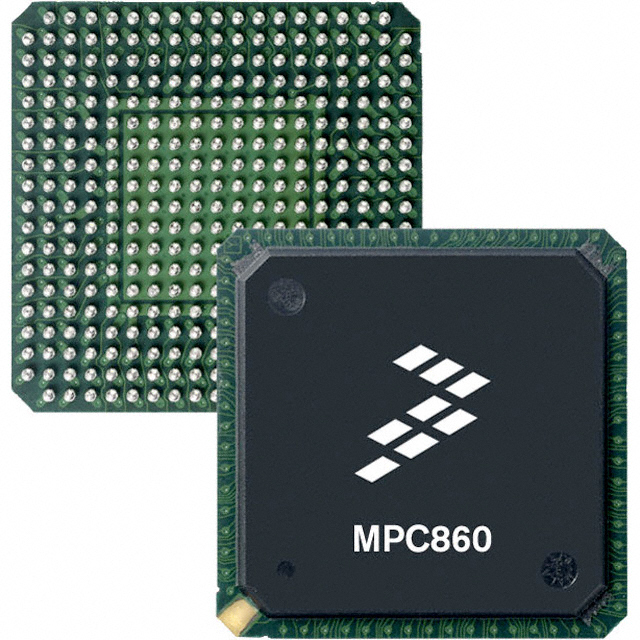
MPC8xx Microprocessor IC MPC8xx 1 Core, 32-Bit 133MHz 256-PBGA (23x23) |
|---|---|
| Quantity | 627 Available (as of October 8, 2026) |
| Product Category | Microprocessors |
|---|---|
| Part Series | MPC875 |
| Manufacturer | NXP USA Inc. |
| Manufacturing Status | Obsolete |
| Manufacturer Standard Lead Time | Contact Us |
| Datasheet |
Specifications & Environmental
| Co-Processors/DSP | Communications; CPM, Security; SEC | Core Processor | MPC8xx | Device Package | 256-PBGA (23x23) | ||
|---|---|---|---|---|---|---|---|
| ECCN | 5A002A1 FRE | Ethernet | 10Mbps (1), 10/100Mbps (2) | Graphics Acceleration | No | ||
| HTS Code | 8542.31.0001 | Moisture Sensitivity Level | 3 (168 Hours) | Mounting Method | Surface Mount | ||
| Mounting Type | Surface Mount | Number of Cores/Bus Width | 1 Core, 32-Bit | Operating Temperature | 0°C ~ 95°C (TA) | ||
| Package / Case | 256-BBGA | RAM Controllers | DRAM | REACH Compliance | REACH Unaffected | ||
| RoHS Compliance | ROHS3 Compliant | Security Features | Cryptography | Speed | 133MHz | ||
| Supplier Device Package | 256-PBGA (23×23) | USB | USB 2.0 (1) | Voltage – I/O | 3.3V |
Overview of KMPC875VR133 – IC MPU MPC8XX 133MHZ 256BGA
The KMPC875VR133 is a single‑chip microprocessor built around the MPC8xx 32‑bit core running at 133 MHz. Designed for embedded controller and communications applications, the device integrates a system integration unit (SIU), a communications processor module (CPM), and security functionality to simplify system design.
With integrated Ethernet interfaces, USB 2.0 support, DRAM controller capability and hardware cryptography, the KMPC875VR133 targets communications and networking systems, embedded controllers and other consumer‑grade embedded applications that require on‑chip peripheral integration and deterministic performance.
Key Features
- Core and Architecture Single 32‑bit MPC8xx core at 133 MHz; Power Architecture™ based CPU with single‑issue pipeline, 32×32‑bit general purpose registers, and branch prediction with conditional prefetch.
- Instruction and Data Caches On‑chip caches include an 8 KB instruction cache and an 8 KB data cache to improve code and data throughput for embedded workloads.
- System Integration Integrated system integration unit (SIU) and communications processor module (CPM) provide on‑chip support for communication protocols and peripheral control.
- Communications and Interfaces Multiple Ethernet interfaces (one 10 Mbps port and two 10/100 Mbps ports), USB 2.0 (1), and HDLC/SDLC support for industry interfaces and protocol handling.
- Security and Offload On‑chip security/cryptography engine (SEC) and communications co‑processor (CPM) to accelerate secure communications and protocol processing.
- Memory and Bus DRAM controller support and external bus operation; the external bus supports up to 80 MHz in 1:1 mode while the 133 MHz core operates in 2:1 mode.
- Power and IO 3.3 V I/O signaling for common embedded system levels.
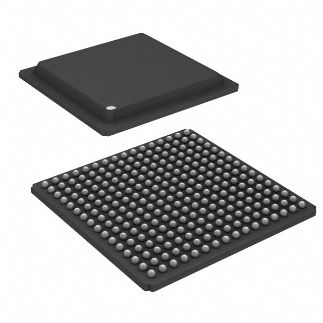
- Package and Mounting 256‑pin PBGA package (23 × 23 mm), surface‑mount configuration suitable for compact board designs.
- Operating Range and Qualification Consumer qualification with an operating temperature range of 0 °C to 95 °C and RoHS compliance.
Typical Applications
- Communications & Networking: Use as a protocol and packet‑processing controller in routers, gateways and access devices leveraging the CPM, multiple Ethernet ports and hardware cryptography.
- Embedded Controllers: Integration of core, SIU and peripheral engines makes the part suitable for controller applications that require DRAM support and multiple serial/HDLC interfaces.
- Secure Networking Appliances: On‑chip SEC cryptography and CPM offload enable secure data handling and protocol acceleration for consumer networking equipment.
Unique Advantages
- Highly integrated communications peripherals: Built‑in CPM, multiple Ethernet ports and USB 2.0 reduce external component count and simplify board design.
- Power Architecture core with caches: 32‑bit MPC8xx core with 8 KB instruction and 8 KB data caches improves execution efficiency for embedded code.
- Designed for embedded networking use: External bus support, DRAM controller and HDLC/SDLC interfaces enable common embedded networking topologies.
- Compact PBGA package: 256‑pin PBGA (23 × 23 mm) provides a balance of IO density and compact footprint for space‑constrained designs.
- Standards‑oriented IO levels and compliance: 3.3 V I/O and RoHS compliance facilitate integration into modern consumer electronic assemblies.
Why Choose KMPC875VR133?
The KMPC875VR133 combines a Power Architecture™ MPC8xx core with integrated system and communications modules to deliver a compact, single‑chip solution for embedded communication and controller applications. Its mix of Ethernet ports, USB 2.0, DRAM controller capability and on‑chip cryptography is aimed at developers who need integrated peripherals and protocol offload without adding multiple discrete controllers.
Backed by NXP Semiconductors’ MPC875 family documentation and hardware specifications, the KMPC875VR133 is well suited for consumer‑grade networking and embedded designs that prioritize integration, determinism and a streamlined BOM.
Request a quote or submit an inquiry to get pricing and availability for KMPC875VR133.





















Date Founded: 2006
Headquarters: Eindhoven, North Brabant, Netherlands
Employees: 38,000+
Revenue: $10.53 Billion
Certifications and Memberships: ISO9001:2015, IATF16949:2016


