
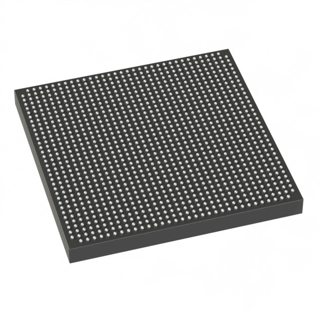
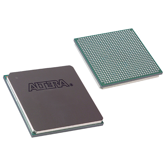
EP2SGX60DF780C5N
| Part Description |
Stratix® II GX Field Programmable Gate Array (FPGA) IC 364 2544192 60440 780-BBGA |
|---|---|
| Quantity | 845 Available (as of June 18, 2026) |

| Product Category | Field Programmable Gate Array (FPGA) |
|---|---|
| Manufacturer | Intel |
| Manufacturing Status | Obsolete |
| Manufacturer Standard Lead Time | Contact Us |
| Datasheet |
Specifications & Environmental
| Device Package | 780-FBGA (29x29) | Grade | Commercial | Operating Temperature | 0°C – 85°C | ||
|---|---|---|---|---|---|---|---|
| Package / Case | 780-BBGA | Number of I/O | 364 | Voltage | 1.15 V - 1.25 V | ||
| Mounting Method | Surface Mount | RoHS Compliance | RoHS Compliant | REACH Compliance | REACH Unaffected | ||
| Moisture Sensitivity Level | 3 (168 Hours) | Number of LABs/CLBs | 3022 | Number of Logic Elements/Cells | 60440 | ||
| Number of Gates | N/A | ECCN | 3A991D | HTS Code | 8542.39.0001 | ||
| Qualification | N/A | Total RAM Bits | 2544192 |
Overview of EP2SGX60DF780C5N – Stratix® II GX Field Programmable Gate Array (FPGA) IC
The EP2SGX60DF780C5N is a Stratix® II GX family FPGA in a 780-ball BGA package, designed for high-performance, reprogrammable logic and I/O integration. It combines a large logic array and embedded memory with the Stratix II GX family’s high-speed serial transceiver architecture to address high-speed backplane, chip-to-chip, and communications bridging applications.
Built for commercial-grade systems, this device provides a balance of dense logic resources, significant on-chip RAM, wide I/O count, and low-voltage operation to support complex digital designs and protocol-centric implementations.
Key Features
- Logic Capacity Provides 60,440 logic elements across 3,022 LABs to implement complex digital functions and state machines.
- Embedded Memory Approximately 2.54 Mbits of on-chip RAM suitable for FIFOs, buffering, and on-chip data storage.
- I/O Density 364 user I/O pins to support broad interface requirements and parallel I/O buses.
- Stratix II GX Transceiver Architecture (family-level) Stratix II GX devices include high-speed serial transceivers with clock and data recovery and SERDES capabilities supporting data rates up to 6.375 Gbps per channel (family feature).
- Clocking and DSP Resources (family-level) Family-level features include up to four enhanced PLLs and dedicated high-speed DSP blocks for multiplier and MAC implementations (as described in the Stratix II GX device documentation).
- Power and Supply Operates from a core supply range of 1.15 V to 1.25 V for the logic array.
- Package 780-ball BGA (supplier package: 780-FBGA, 29 × 29 mm) for compact, high-density board implementations.
- Grade and Temperature Commercial grade with an operating temperature range of 0 °C to 85 °C.
- Standards & Integration (family-level) Stratix II GX family documentation describes support for multiple I/O standards, selectable on-chip termination, adaptive equalization, and dynamic transceiver configuration (family-level features).
- RoHS Compliance Device is RoHS compliant.
Typical Applications
- Telecommunications & Networking High-speed serial links and on-chip logic make this device suitable for protocol bridging, packet processing, and backplane interfaces.
- High-speed I/O Systems Large I/O count and family transceiver capabilities support multi-channel, source-synchronous, and serial interface designs.
- Signal Processing & Compute Acceleration Significant logic resources and embedded memory enable implementation of DSP pipelines, buffering, and custom compute blocks.
- Board-level Integration Dense BGA packaging and extensive I/O allow the FPGA to consolidate functions and reduce external component count on complex PCBs.
Unique Advantages
- High logic density: 60,440 logic elements provide headroom for complex control, protocol handling, and custom accelerators.
- Substantial on-chip memory: Approximately 2.54 Mbits of embedded RAM for FIFOs, buffering, and low-latency data paths without external memory.
- Versatile I/O resources: 364 I/O pins support diverse parallel and serial interfaces, simplifying board-level connectivity.
- Family-level transceiver capability: Stratix II GX family transceivers offer high-speed serial data rates and CDR/SERDES functionality for high-bandwidth links.
- Compact, manufacturable package: 780-ball BGA (29 × 29) balances pin count and PCB real estate for production designs.
- Commercial-grade qualification: Rated for 0 °C to 85 °C operation to match standard commercial system environments.
Why Choose EP2SGX60DF780C5N?
EP2SGX60DF780C5N combines a large, scalable logic array and meaningful embedded memory with the Stratix II GX family’s high-speed transceiver architecture to address demanding digital and protocol-focused designs. Its mix of logic density, I/O capacity, and BGA packaging makes it appropriate for systems that require integration of complex logic, buffering, and high-speed links in a commercial-temperature environment.
For engineering teams building communications, backplane, or high-performance embedded systems, this device offers a platform that aligns performance-oriented architecture with the documented Stratix II GX family features and Intel’s device-level specifications.
Request a quote or submit an inquiry to receive pricing, availability, and additional technical support for EP2SGX60DF780C5N.


Date Founded: 1968
Headquarters: Santa Clara, California, USA
Employees: 130,000+
Revenue: $54.23 Billion
Certifications and Memberships: ISO9001:2015, ISO14001:2015, ISO17025:2017, ISO27001:2022, ISO45001:2018, ISO50001:2018


