
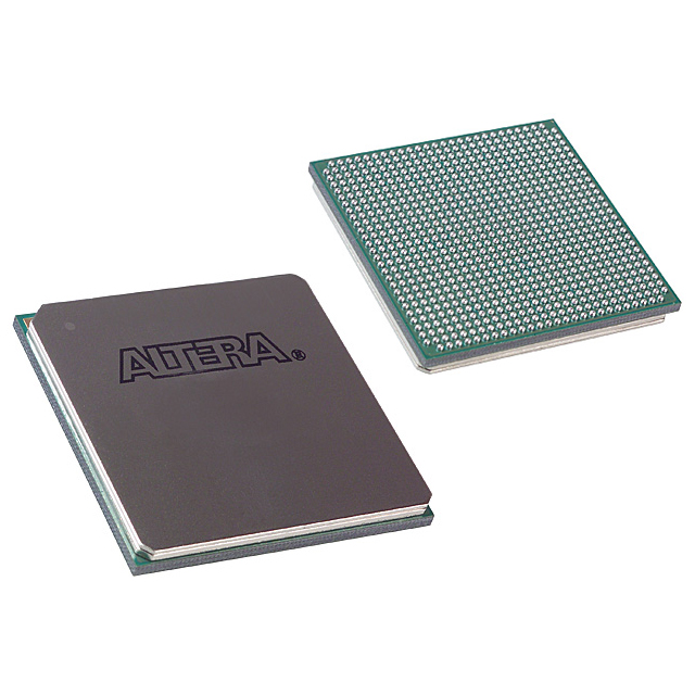
EP2SGX60EF1152C3N
| Part Description |
Stratix® II GX Field Programmable Gate Array (FPGA) IC 534 2544192 60440 1152-BBGA |
|---|---|
| Quantity | 54 Available (as of June 14, 2026) |

| Product Category | Field Programmable Gate Array (FPGA) |
|---|---|
| Manufacturer | Intel |
| Manufacturing Status | Obsolete |
| Manufacturer Standard Lead Time | Contact Us |
| Datasheet |
Specifications & Environmental
| Device Package | 1152-FBGA (35x35) | Grade | Commercial | Operating Temperature | 0°C – 85°C | ||
|---|---|---|---|---|---|---|---|
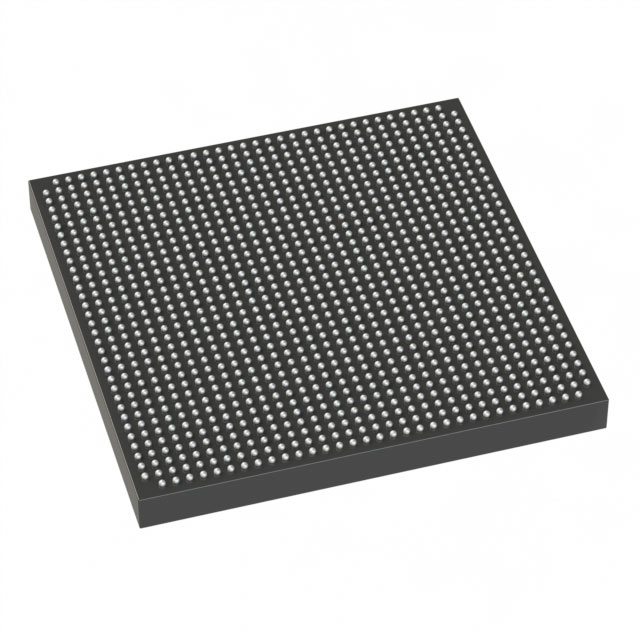
| Package / Case | 1152-BBGA | Number of I/O | 534 | Voltage | 1.15 V - 1.25 V | ||
| Mounting Method | Surface Mount | RoHS Compliance | RoHS Compliant | REACH Compliance | REACH Unaffected | ||
| Moisture Sensitivity Level | 3 (168 Hours) | Number of LABs/CLBs | 3022 | Number of Logic Elements/Cells | 60440 | ||
| Number of Gates | N/A | ECCN | 3A001A7A | HTS Code | 8542.39.0001 | ||
| Qualification | N/A | Total RAM Bits | 2544192 |
Overview of EP2SGX60EF1152C3N – Stratix® II GX Field Programmable Gate Array (FPGA) IC 534 2544192 60440 1152-BBGA
The EP2SGX60EF1152C3N is a Stratix® II GX family FPGA delivering a high-density, high-performance programmable fabric for demanding communications and system-integration designs. Built on the Stratix II GX architecture, the device couples a large logic array with substantial embedded memory and a dense I/O footprint to address high-speed backplane, chip-to-chip, and protocol-bridging applications.
This surface-mount 1152-ball BGA device provides 60,440 logic elements, approximately 2.54 Mbits of embedded memory, and 534 general-purpose I/O pins, all optimized for scalable performance, flexible interfacing, and integration in commercial-temperature systems.
Key Features
- Logic Capacity — 60,440 logic elements for implementing complex state machines, protocol stacks, and custom datapaths.
- Embedded Memory — Approximately 2.54 Mbits of on-chip RAM to implement FIFOs, buffers, and on-chip data storage without external memory in many designs.
- I/O Density — 534 I/O pins delivered in a high-density package to support wide parallel buses, multiple peripherals, and high-channel-count interfaces.
- High‑Speed Transceiver Architecture (Series Feature) — Stratix II GX family devices include high-speed serial transceivers supporting up to 6.375 Gbps and protocol flexibility for communications links and backplane interfaces.
- DSP and Clocking (Series Feature) — Integrated high-speed DSP blocks and multiple PLLs provide dedicated multiply-accumulate performance and advanced clock management for signal processing and timing-critical designs.
- Package & Mounting — 1152-BBGA (supplier package: 1152-FBGA, 35×35 mm) surface-mount package for compact, high-density board integration.
- Power Supply — Core supply range 1.15 V to 1.25 V for the device core.
- Operating Range & Grade — Commercial temperature grade specified 0 °C to 85 °C.
- Environment — RoHS compliant.
Typical Applications
- High-Speed Backplane Interfaces — Use the Stratix II GX architecture’s serial transceiver capability and dense logic to implement backplane bridging and packet switching functions.
- Chip-to-Chip Communications — Leverage the device’s large logic array and high I/O count for protocol conversion and low-latency bridging between silicon components.
- Telecom & Networking Equipment — Implement protocol processing, aggregation, and buffering with the on-chip RAM and DSP resources available in the Stratix II GX family.
- Custom High-Performance Controllers — Create specialized control and signal-processing blocks that require many logic elements, embedded memory, and flexible clocking.
Unique Advantages
- High Integration: 60,440 logic elements and ~2.54 Mbits of embedded memory consolidate functionality on-chip, reducing external components and board complexity.
- Dense I/O Footprint: 534 I/O pins in a 1152-ball BGA package enable broad peripheral and bus connectivity while maintaining a compact PCB footprint.
- Family-Level High-Speed Transceivers: Stratix II GX devices provide transceiver technology supporting multi‑Gbps links, giving designers access to adaptable serial connectivity for communications applications.
- Flexible Clocking and DSP Resources: On-chip DSP blocks and multiple PLLs support compute-intensive and timing-sensitive functions directly in the FPGA fabric.
- Commercial Temperature Suitability: Rated for 0 °C to 85 °C operation to meet the needs of standard commercial electronic products.
- Regulatory Compliance: RoHS compliant for global manufacturing and environmental requirements.
Why Choose EP2SGX60EF1152C3N?
The EP2SGX60EF1152C3N places a large, flexible Stratix II GX FPGA into a compact BGA footprint, combining substantial logic capacity, embedded memory, and a high I/O count for designs that require both compute density and extensive interfacing. It is positioned for engineers building communications, protocol conversion, and high-performance controller systems who need a programmable, scalable solution backed by the Stratix II GX device architecture.
Choosing this device delivers long-term design scalability through a platform that supports high-speed serial links, dedicated DSP resources, and advanced clocking. The combination of on-chip resources, commercial-grade temperature support, and RoHS compliance makes it suitable for many production electronic systems where integration and performance are priorities.
Request a quote or submit an inquiry to receive pricing and availability for the EP2SGX60EF1152C3N and to discuss how this Stratix II GX FPGA can meet your design requirements.


Date Founded: 1968
Headquarters: Santa Clara, California, USA
Employees: 130,000+
Revenue: $54.23 Billion
Certifications and Memberships: ISO9001:2015, ISO14001:2015, ISO17025:2017, ISO27001:2022, ISO45001:2018, ISO50001:2018


