
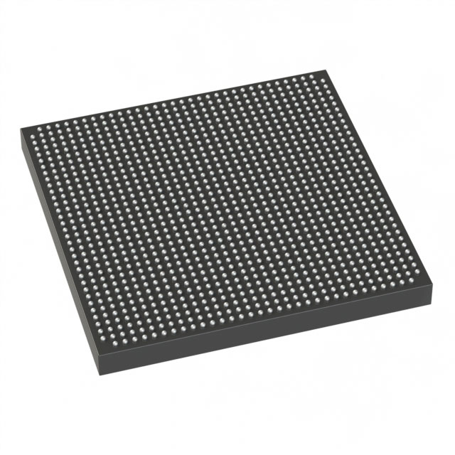
EP2SGX60EF1152C5N
| Part Description |
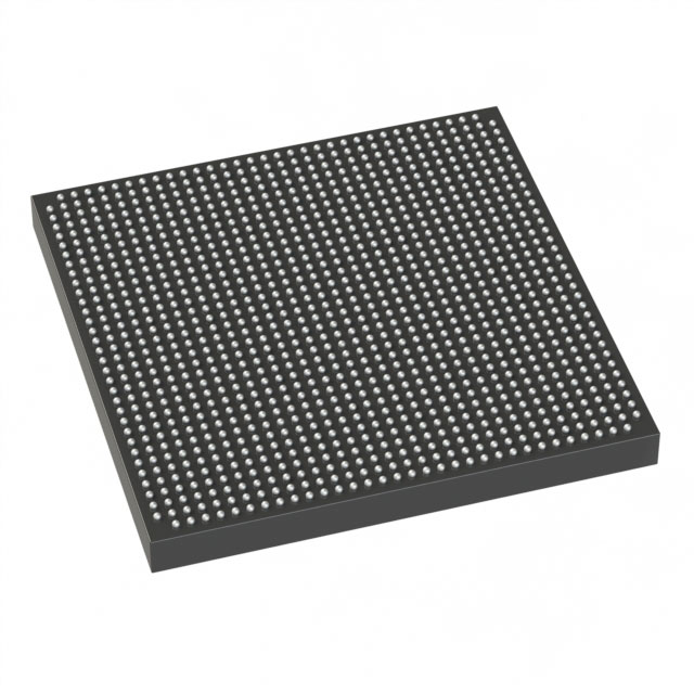
Stratix® II GX Field Programmable Gate Array (FPGA) IC 534 2544192 60440 1152-BBGA |
|---|---|
| Quantity | 48 Available (as of October 7, 2026) |
| Product Category | Field Programmable Gate Array (FPGA) |
|---|---|
| Manufacturer | Intel |
| Manufacturing Status | Obsolete |
| Manufacturer Standard Lead Time | Contact Us |
| Datasheet |
Specifications & Environmental
| Device Package | 1152-FBGA (35x35) | Grade | Commercial | Operating Temperature | 0°C – 85°C | ||
|---|---|---|---|---|---|---|---|
| Package / Case | 1152-BBGA | Number of I/O | 534 | Voltage | 1.15 V - 1.25 V | ||
| Mounting Method | Surface Mount | RoHS Compliance | RoHS Compliant | REACH Compliance | REACH Unaffected | ||
| Moisture Sensitivity Level | 3 (168 Hours) | Number of LABs/CLBs | 3022 | Number of Logic Elements/Cells | 60440 | ||
| Number of Gates | N/A | ECCN | 3A001A7A | HTS Code | 8542.39.0001 | ||
| Qualification | N/A | Total RAM Bits | 2544192 |
Overview of EP2SGX60EF1152C5N – Stratix® II GX FPGA 1152-BBGA
The EP2SGX60EF1152C5N is a Stratix II GX field-programmable gate array (FPGA) in a 1152-ball BGA package, offering a scalable logic array combined with the Stratix II GX family's high-speed serial transceiver architecture. This device targets applications that require dense logic, substantial embedded memory, and advanced serial connectivity for communications and interface bridging.
Key device attributes include 60,440 logic elements, approximately 2.54 Mbits of on-chip RAM, 534 I/O pins, a 1152-ball FBGA (35×35) package, and a 1.15 V to 1.25 V supply range. The device is graded for commercial use with an operating temperature range of 0 °C to 85 °C and is RoHS compliant.
Key Features
- Logic Density Provides 60,440 logic elements to implement complex, high-density digital functions and custom logic subsystems.
- Embedded Memory Approximately 2.54 Mbits of on-chip RAM (2,544,192 bits) for FIFOs, buffers, and temporary storage.
- I/O Capacity 534 I/O pins support extensive external interfacing and parallel bus connectivity in a single device.
- High‑Speed Serial Transceivers (Stratix II GX family) Family-level transceiver capabilities include channels operating from 600 Mbps up to 6.375 Gbps and device options with 4 to 20 channels, enabling high-bandwidth serial links and protocol bridging.
- Clocking and DSP Stratix II GX family features include up to four enhanced PLLs with advanced reconfiguration and high-speed DSP blocks that support multipliers and multiply-accumulate functions (DSP multiplier performance up to 450 MHz as specified for the family).
- Memory and Bus Support (family-level) TriMatrix memory architecture (three RAM block sizes) and support for high-speed external memory interfaces help implement true dual-port memories and FIFOs with high performance.
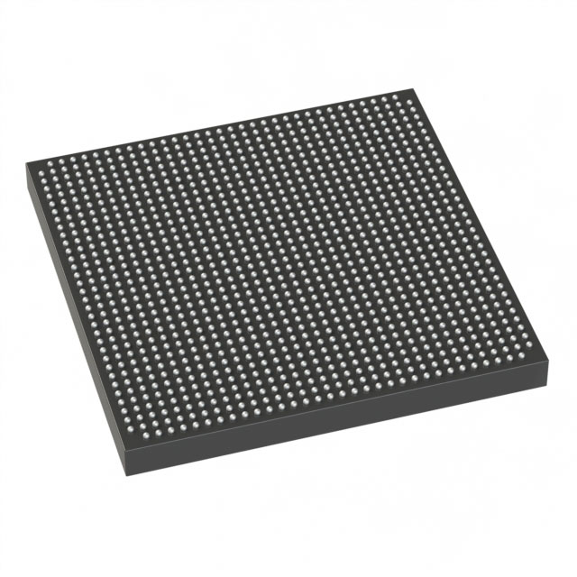
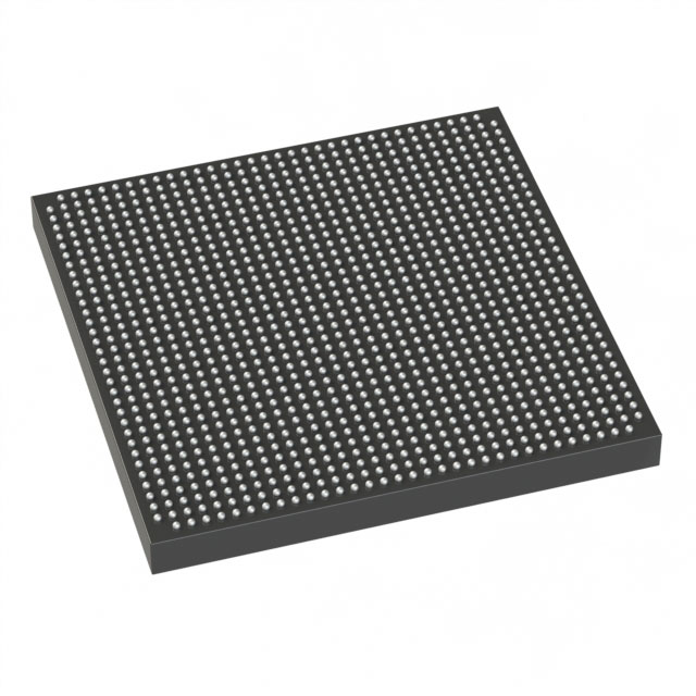
- Package & Mounting Supplied in a 1152-FBGA (35×35) package for surface-mount assembly, suitable for compact board designs that require high pin count and signal density.
- Power & Temperature Operates from a 1.15 V to 1.25 V supply and is specified for commercial temperature operation from 0 °C to 85 °C.
- Compliance RoHS compliant for environmental compatibility in commercial applications.
Typical Applications
- High‑speed communications Used for protocol bridging and high-bandwidth serial links where Stratix II GX transceiver capabilities (up to 6.375 Gbps) and large logic density are required.
- Backplane and chip‑to‑chip interfaces Implements complex backplane protocols and chip-to-chip connectivity leveraging the device’s abundant I/O and serial transceiver options.
- Packet processing and switching Embeds buffering and packet-handling logic using the device’s substantial on-chip RAM and DSP resources for acceleration of data-path functions.
- Custom FPGA compute and signal processing Supports DSP-heavy functions through on-chip DSP blocks and the large logic array for multiply-accumulate and FIR implementations.
Unique Advantages
- High logic capacity: 60,440 logic elements enable dense implementation of complex digital systems and IP cores without partitioning across multiple devices.
- Significant embedded memory: Approximately 2.54 Mbits of on-chip RAM reduces external memory dependence for FIFOs, buffering, and shared storage.
- Extensive I/O availability: 534 I/O pins provide flexibility for wide buses, parallel interfaces, and high pin-count peripherals on a single FPGA.
- Advanced serial connectivity (family-level): Stratix II GX transceivers support multi-gigabit links and dynamic protocol reconfiguration to address a range of serial communication standards.
- Compact, high-density packaging: 1152-FBGA (35×35) package offers a high pin count in a compact form factor for space-constrained boards.
- Commercial-grade and compliant: Commercial operating range (0 °C to 85 °C) and RoHS compliance suitable for mainstream electronic products.
Why Choose EP2SGX60EF1152C5N?
The EP2SGX60EF1152C5N combines the Stratix II GX family's high-speed serial capabilities with substantial logic density and embedded memory, making it a practical choice for designs that require integrated high-bandwidth links alongside complex logic and buffering. Its 1152-ball FBGA package and large I/O count simplify board-level integration where signal density and compactness matter.
This device is well suited for engineering teams building communications interfaces, backplane and chip-to-chip solutions, or compute-accelerated FPGA subsystems that benefit from on-chip RAM and DSP resources. The combination of family-level transceiver features, device-level resources, and commercial-grade specifications delivers a scalable platform backed by existing Stratix II GX device definitions and documentation.
Request a quote or submit an inquiry to discuss availability, pricing, or to get technical procurement assistance for the EP2SGX60EF1152C5N.





















Date Founded: 1968
Headquarters: Santa Clara, California, USA
Employees: 130,000+
Revenue: $54.23 Billion
Certifications and Memberships: ISO9001:2015, ISO14001:2015, ISO17025:2017, ISO27001:2022, ISO45001:2018, ISO50001:2018


