
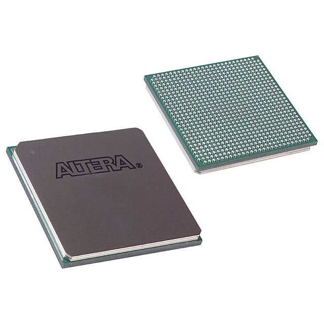
EP2SGX60EF1152C4N
| Part Description |
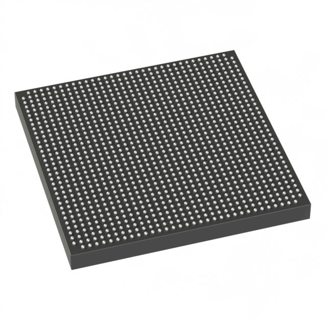
Stratix® II GX Field Programmable Gate Array (FPGA) IC 534 2544192 60440 1152-BBGA |
|---|---|
| Quantity | 600 Available (as of June 14, 2026) |

| Product Category | Field Programmable Gate Array (FPGA) |
|---|---|
| Manufacturer | Intel |
| Manufacturing Status | Obsolete |
| Manufacturer Standard Lead Time | Contact Us |
| Datasheet |
Specifications & Environmental
| Device Package | 1152-FBGA (35x35) | Grade | Commercial | Operating Temperature | 0°C – 85°C | ||
|---|---|---|---|---|---|---|---|
| Package / Case | 1152-BBGA | Number of I/O | 534 | Voltage | 1.15 V - 1.25 V | ||
| Mounting Method | Surface Mount | RoHS Compliance | RoHS Compliant | REACH Compliance | REACH Unaffected | ||
| Moisture Sensitivity Level | 3 (168 Hours) | Number of LABs/CLBs | 3022 | Number of Logic Elements/Cells | 60440 | ||
| Number of Gates | N/A | ECCN | 3A001A7A | HTS Code | 8542.39.0001 | ||
| Qualification | N/A | Total RAM Bits | 2544192 |
Overview of EP2SGX60EF1152C4N – Stratix® II GX Field Programmable Gate Array (FPGA) IC 534 2544192 60440 1152-BBGA
The EP2SGX60EF1152C4N is a Stratix® II GX family FPGA in a 1152‑ball BGA package designed for high-performance, high‑density programmable logic applications. It combines a large logic array and substantial on‑chip memory with the Stratix II GX family’s high‑speed serial transceiver architecture.
This device is targeted at high‑bandwidth designs such as backplane interfaces, chip‑to‑chip links, and communications protocol bridging where dense logic, abundant I/O, and embedded memory are required. Key value comes from its large logic resource count, multi‑megabit embedded RAM, and Stratix II GX transceiver capabilities described in the device family documentation.
Key Features
- Core Logic — Contains 60,440 logic elements and 3,022 logic array blocks, enabling implementation of complex digital functions and large custom logic engines.
- Embedded Memory — Approximately 2.544 Mbits of on‑chip RAM to support FIFOs, buffers, and data storage without external memory in many designs.
- High‑Speed Transceiver Family Features — Stratix II GX family transceiver architecture supports clock‑data recovery and SERDES operation up to 6.375 Gbps (family specification), enabling high‑bandwidth serial links and protocol bridging.
- I/O and Interfaces — 534 user I/O pins to support wide parallel buses, multiple interfaces, and high pin‑count connectivity options.
- Package & Mounting — 1152‑FBGA (35 × 35 mm) package, surface‑mountable for compact board designs and high pin density.
- Power — Operates from a core voltage range of 1.15 V to 1.25 V consistent with Stratix II GX logic core requirements.
- Operating Range & Compliance — Commercial grade with an operating temperature range of 0 °C to 85 °C and RoHS compliance for environmental regulation alignment.
- Family‑Level Functionality — Stratix II GX device family supports advanced on‑chip DSP blocks, multiple PLLs, configurable I/O standards, and IP megafunction support as described in the device family documentation.
Typical Applications
- High‑speed backplane interfaces — Use the device’s family transceiver capabilities and dense logic to implement multiplexing, framing, and protocol handling for backplane links.
- Chip‑to‑chip communications — Implement high‑bandwidth serialized links and parallel interface bridging between ASICs, processors, and memory subsystems.
- Communications protocol bridging — Translate and bridge between serial protocols and parallel buses leveraging on‑chip logic, embedded RAM, and transceiver functionality.
- High‑performance buffering and packet processing — Leverage approximately 2.544 Mbits of embedded RAM and substantial logic resources for packet buffering, queuing, and custom packet processing engines.
Unique Advantages
- High logic density: 60,440 logic elements provide the resources needed for large custom logic implementations and multi‑function designs.
- Significant on‑chip memory: Approximately 2.544 Mbits of embedded RAM reduces reliance on external memory for many buffering and FIFO requirements, simplifying BOM and board complexity.
- Built on Stratix II GX transceiver architecture: Family transceiver support to 6.375 Gbps enables high‑bandwidth serial links and flexible protocol support for communications applications.
- Broad I/O count: 534 I/O pins support extensive external connectivity for complex systems and wide data buses.
- Compact, high‑pin‑count packaging: 1152‑FBGA (35 × 35 mm) package provides dense routing and mounting for space‑constrained, high‑performance PCBs.
- Commercial grade and RoHS compliant: Rated for 0 °C to 85 °C operation and RoHS compliance for standard commercial deployments.
Why Choose EP2SGX60EF1152C4N?
The EP2SGX60EF1152C4N positions itself where high logic capacity, multi‑megabit embedded memory, and Stratix II GX family transceiver capability are required. Its combination of 60,440 logic elements, approximately 2.544 Mbits of RAM, and 534 I/Os supports complex protocol handling, buffering, and high‑bandwidth connectivity within a compact 1152‑ball BGA footprint.
This device suits engineering teams building high‑bandwidth communications, backplane, and chip‑to‑chip systems that need scalable logic resources and family‑level transceiver features. The Stratix II GX family documentation also describes supported IP, PLL capabilities, and configuration features that support integration and long‑term design scalability.
Request a quote or submit an inquiry to discuss availability, lead times, and pricing for EP2SGX60EF1152C4N and to get assistance matching this FPGA to your project requirements.


Date Founded: 1968
Headquarters: Santa Clara, California, USA
Employees: 130,000+
Revenue: $54.23 Billion
Certifications and Memberships: ISO9001:2015, ISO14001:2015, ISO17025:2017, ISO27001:2022, ISO45001:2018, ISO50001:2018


