
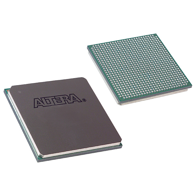
EP2SGX60EF1152C4
| Part Description |
Stratix® II GX Field Programmable Gate Array (FPGA) IC 534 2544192 60440 1152-BBGA |
|---|---|
| Quantity | 469 Available (as of June 15, 2026) |

| Product Category | Field Programmable Gate Array (FPGA) |
|---|---|
| Manufacturer | Intel |
| Manufacturing Status | Obsolete |
| Manufacturer Standard Lead Time | Contact Us |
| Datasheet |
Specifications & Environmental
| Device Package | 1152-FBGA (35x35) | Grade | Commercial | Operating Temperature | 0°C – 85°C | ||
|---|---|---|---|---|---|---|---|
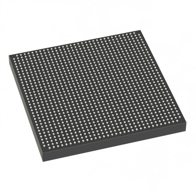
| Package / Case | 1152-BBGA | Number of I/O | 534 | Voltage | 1.15 V - 1.25 V | ||
| Mounting Method | Surface Mount | RoHS Compliance | RoHS non-compliant | REACH Compliance | REACH Unaffected | ||
| Moisture Sensitivity Level | 3 (168 Hours) | Number of LABs/CLBs | 3022 | Number of Logic Elements/Cells | 60440 | ||
| Number of Gates | N/A | ECCN | 3A001A7A | HTS Code | 8542.39.0001 | ||
| Qualification | N/A | Total RAM Bits | 2544192 |
Overview of EP2SGX60EF1152C4 – Stratix® II GX Field Programmable Gate Array (FPGA) IC 534 2544192 60440 1152-BBGA
The EP2SGX60EF1152C4 is a commercial-grade Stratix II GX FPGA offered in a 1152-ball BGA package. It combines a high-performance logic array with the Stratix II GX family’s high-speed serial transceiver architecture to address demanding communications and high-speed interface applications.
Designed for applications that require dense logic, abundant I/O and embedded memory, this device provides 60,440 logic elements, approximately 2.54 Mbits of embedded memory, and 534 user I/Os while operating at a core supply range of 1.15 V to 1.25 V and a commercial temperature range of 0 °C to 85 °C.
Key Features
- Logic Capacity — 60,440 logic elements to implement complex digital functions and system-level integration.
- Embedded Memory — Approximately 2.54 Mbits of on-chip RAM for FIFOs, buffers and on-chip storage.
- I/O and Packaging — 534 user I/Os in a 1152-ball BGA (supplier package: 1152-FBGA, 35 × 35 mm) optimized for high-density, surface-mount board designs.
- Power and Temperature — Core voltage supply range 1.15 V to 1.25 V; commercial operating range 0 °C to 85 °C.
- Transceiver Architecture (family) — Stratix II GX family devices include high-speed serial transceivers with clock and data recovery supporting 600 Mbps to 6.375 Gbps per channel and protocols such as PCI Express and Gigabit Ethernet.
- Memory Architecture (family) — TriMatrix memory structure for multiple RAM block sizes and high-performance true dual-port memories and FIFOs.
- DSP & Clock Resources (family) — Dedicated high-speed DSP blocks and up to 16 global clock networks with regional clocking for timing-critical applications; up to four enhanced PLLs for advanced clocking control.
- Compliance — RoHS compliant; commercial-grade device and surface-mount mounting type.
Typical Applications
- High-speed Networking — Implement protocol bridging and packet processing using the Stratix II GX transceiver family capabilities and dense logic resources.
- Backplane & Chip-to-Chip Interfaces — Support high-bandwidth serial links and parallel interfaces with abundant I/O and embedded memory for buffering and alignment.
- Communications Systems — Enable SERDES-based links and protocol-specific IP cores using the family’s transceiver and clocking features.
- Custom Hardware Acceleration — Use on-chip DSP blocks and large logic capacity to accelerate signal processing and algorithmic functions.
Unique Advantages
- High Logic Density: 60,440 logic elements provide capacity to consolidate multiple functions or large custom datapaths into a single FPGA device.
- Substantial On-chip Memory: Approximately 2.54 Mbits of embedded RAM reduces dependence on external memory for buffering and small data stores.
- Extensive I/O Count: 534 user I/Os in a compact 1152-ball BGA package enables dense connector and peripheral interfacing on modern PCBs.
- Family-Level High-Speed Transceivers: Stratix II GX transceiver technology supports up to 6.375 Gbps per channel and common serial protocols, enabling versatile link options.
- Commercial-Grade Robustness: Rated for 0 °C to 85 °C operation and RoHS compliant for standard commercial electronics deployments.
- Flexible Clocking and DSP Resources: Family features such as multiple global/regional clock networks, enhanced PLLs, and dedicated DSP blocks support performance-focused designs.
Why Choose EP2SGX60EF1152C4?
The EP2SGX60EF1152C4 positions itself as a high-capacity, commercially graded Stratix II GX FPGA that balances dense logic, substantial embedded memory and broad I/O in a 1152-BBGA package. Its core voltage range and temperature rating make it suitable for mainstream communications, networking, and high-speed interface applications that rely on family-level transceiver and DSP capabilities.
Design teams seeking a scalable platform with strong clocking, memory architecture and serial-link support will find this device suited for complex protocol bridging, packet processing and custom hardware acceleration tasks while leveraging the Stratix II GX device family characteristics.
Request a quote or submit a product inquiry to start evaluation or obtain pricing and availability information.


Date Founded: 1968
Headquarters: Santa Clara, California, USA
Employees: 130,000+
Revenue: $54.23 Billion
Certifications and Memberships: ISO9001:2015, ISO14001:2015, ISO17025:2017, ISO27001:2022, ISO45001:2018, ISO50001:2018


