
LS1020ASN7MQB
| Part Description |
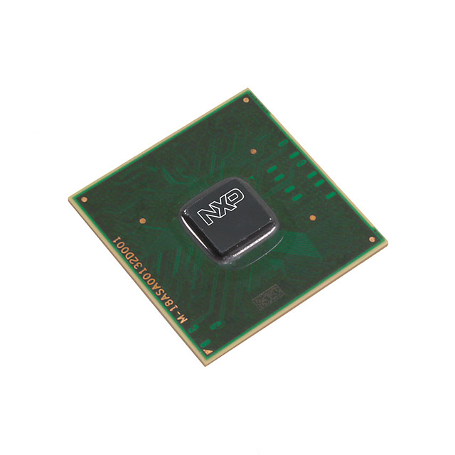
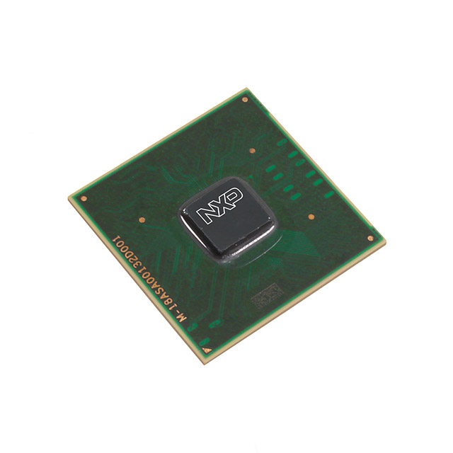
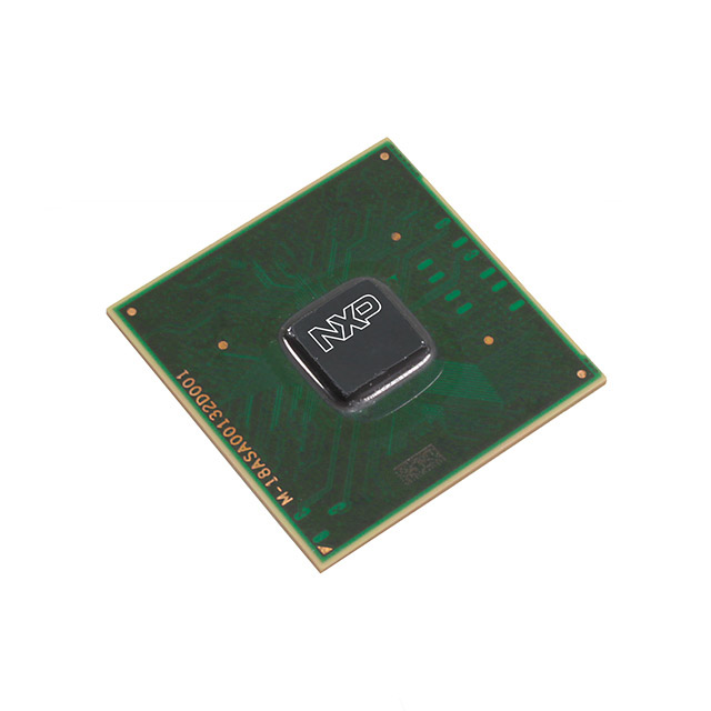
ARM® Cortex®-A7 Microprocessor IC QorIQ® Layerscape 2 Core, 32-Bit 1.2GHz 525-FCPBGA (19x19) |
|---|---|
| Quantity | 1,011 Available (as of October 8, 2026) |

| Product Category | Microprocessors |
|---|---|
| Part Series | LS1020A |
| Manufacturer | NXP USA Inc. |
| Manufacturing Status | Active |
| Manufacturer Standard Lead Time | 18 Weeks |
| Datasheet |
Specifications & Environmental
| Co-Processors/DSP | Multimedia; NEON™ SIMD | Core Processor | ARM® Cortex®-A7 | Device Package | 525-FCPBGA (19x19) | ||
|---|---|---|---|---|---|---|---|
| ECCN | PENDING ECCN | Ethernet | GbE (3) | HTS Code | 0000.00.0000 | ||
| Moisture Sensitivity Level | 3 (168 Hours) | Mounting Method | Surface Mount | Mounting Type | Surface Mount | ||
| Number of Cores/Bus Width | 2 Core, 32-Bit | Operating Temperature | 0°C ~ 105°C | Package / Case | 525-FBGA, FCBGA | ||
| RAM Controllers | DDR3L, DDR4 | REACH Compliance | REACH Unaffected | RoHS Compliance | ROHS3 Compliant | ||
| SATA | SATA 3Gbps (1) | Security Features | Secure Boot, TrustZone® | Speed | 1.2GHz | ||
| Supplier Device Package | 525-FCPBGA (19×19) | USB | USB 2.0 (1), USB 3.0 + PHY |
Overview of LS1020ASN7MQB – IC MPU QORIQ 1.2GHZ 525FCPBGA
The LS1020ASN7MQB is an NXP QorIQ Layerscape microprocessor IC featuring dual ARM® Cortex®-A7 cores running up to 1.2 GHz in a 525-FCPBGA (19×19) package. It targets power-sensitive networking and industrial applications by combining multicore performance with a broad set of high-speed serial interfaces and integrated security.
Designed for embedded networking, gateway and edge designs, the device emphasizes integration and energy-efficient operation, with ECC-protected caches, advanced connectivity options and memory controller support for DDR3L and DDR4 devices.
Key Features
- Core and Performance – Dual ARM® Cortex®-A7 cores, 32-bit, up to 1.2 GHz with ECC-protected L1 and shared L2 caches (32 KB L1 instruction/data per core; up to 512 KB coherent L2).
- Multimedia and Co-processing – Integrated NEON™ SIMD and dual-precision floating-point support for multimedia and DSP-style workloads.
- Memory – On-chip controllers for DDR3L and DDR4 memory types, supporting multiple device widths and throughput suitable for embedded networking stacks.
- High-speed Connectivity – Four-lane, 6 GHz multi-protocol SerDes enabling up to three Gigabit Ethernet ports (with IEEE 1588 support), dual DMA-controlled PCI Express® Gen2 ports and a single SATA 3.0 port.
- USB and Storage – Dual USB controllers including one USB 3.0 controller with integrated PHY plus USB 2.0 support for peripheral connectivity and host functions.
- Security – Secure Boot and ARM TrustZone® to enable hardware-backed platform security and trusted execution.
- Reliability – ECC protection for L1 and L2 caches with single-bit error detect and correction to improve system robustness.
- Package and Thermal – 525-FCPBGA (19×19) surface-mount package; operating temperature range 0°C to 105°C.
- Power-efficient Design – Engineered to deliver multicore performance with a system-level power profile suitable for sub-3 W operation in many use cases.
- Regulatory – RoHS compliant; consumer qualification.
Typical Applications
- Enterprise Access Points – Platform compute and packet processing for 802.11ac/n access points where dual-core throughput and integrated Ethernet are required.
- IoT Gateways – Edge gateway compute, protocol aggregation and secure device connectivity using built-in USB, Gigabit Ethernet and security features.
- Security Appliances – Packet inspection and secure boot-capable gateway designs leveraging TrustZone® and ECC-protected caches for resilient operation.
- I/O Line Cards and Controllers – Embedded controller roles requiring PCIe, SATA and multiple SerDes-based interfaces in a compact BGA package.
Unique Advantages
- Highly integrated connectivity: Multiple Gigabit Ethernet ports, PCIe Gen2, SATA and USB 3.0 with integrated PHY reduce external components and simplify board routing.
- Balanced multicore performance and efficiency: Dual Cortex-A7 cores at up to 1.2 GHz provide multi-threaded application throughput while supporting a low system power envelope.
- Hardware-level security: Secure Boot and ARM TrustZone® enable secure platform initialization and isolated execution for trusted services.
- Memory flexibility: Support for DDR3L and DDR4 device interfaces accommodates a range of system memory configurations and performance targets.
- Robust system reliability: ECC protection on L1 and L2 caches with single-bit error correction improves uptime for embedded networking and industrial deployments.
- Compact production-ready package: 525-FCPBGA surface-mount package and RoHS compliance for streamlined manufacturing and assembly.
Why Choose LS1020ASN7MQB?
The LS1020ASN7MQB combines dual ARM® Cortex®-A7 compute, extensive high-speed serial interfaces and hardware security in a compact, production-ready FCPBGA package. Its integration of SerDes-based networking, PCIe, SATA and USB 3.0 reduces BOM and board complexity while ECC and Secure Boot features support resilient, secure embedded systems.
This device is well suited for engineers building enterprise access points, IoT gateways, security appliances and other networked embedded systems that require balanced performance, low power and a broad peripheral set backed by NXP's QorIQ Layerscape enablement and ecosystem.
Request a quote or submit a sales inquiry to receive pricing, availability and lead-time information for the LS1020ASN7MQB.






















Date Founded: 2006
Headquarters: Eindhoven, North Brabant, Netherlands
Employees: 38,000+
Revenue: $10.53 Billion
Certifications and Memberships: ISO9001:2015, IATF16949:2016


