
LS1026ASN8MQA
| Part Description |
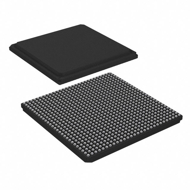
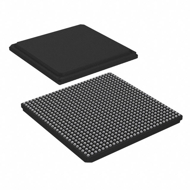
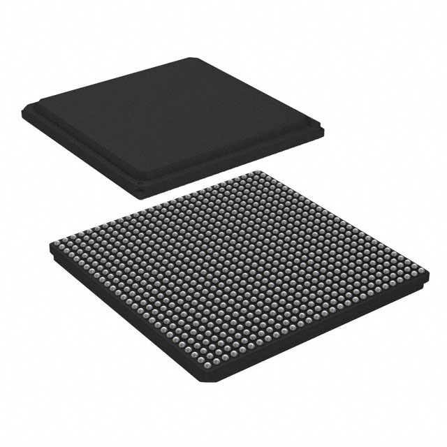
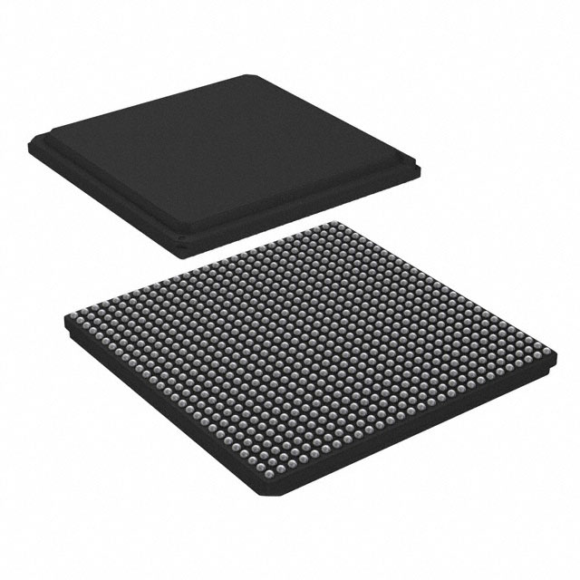
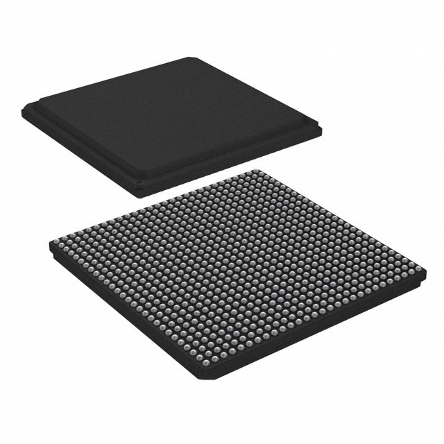
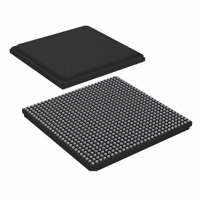
ARM® Cortex®-A72 Microprocessor IC QorIQ® Layerscape 2 Core, 64-Bit 1.2GHz 780-FCPBGA (23x23) |
|---|---|
| Quantity | 575 Available (as of October 8, 2026) |
| Product Category | Microprocessors |
|---|---|
| Part Series | LS1026A |
| Manufacturer | NXP USA Inc. |
| Manufacturing Status | Active |
| Manufacturer Standard Lead Time | 18 Weeks |
| Datasheet |
Specifications & Environmental
| Core Processor | ARM® Cortex®-A72 | Device Package | 780-FCPBGA (23x23) | ECCN | 5A002A1 NXP | ||
|---|---|---|---|---|---|---|---|
| Ethernet | 10GbE (2), 2.5GbE (1), 1GbE (4) | HTS Code | 8542.31.0001 | Moisture Sensitivity Level | 3 (168 Hours) | ||
| Mounting Method | Surface Mount | Mounting Type | Surface Mount | Number of Cores/Bus Width | 2 Core, 64-Bit | ||
| Operating Temperature | 0°C ~ 105°C | Package / Case | 780-FBGA, FCBGA | RAM Controllers | DDR4 | ||
| REACH Compliance | REACH Unaffected | RoHS Compliance | ROHS3 Compliant | SATA | SATA 6Gbps (1) | ||
| Security Features | Secure Boot, TrustZone® | Speed | 1.2GHz | Supplier Device Package | 780-FCPBGA (23×23) | ||
| USB | USB 3.0 (3) + PHY |
Overview of LS1026ASN8MQA – IC MPU QORIQ 1.2GHZ 780FCPBGA
The LS1026ASN8MQA is an NXP QorIQ Layerscape microprocessor featuring dual ARM® Cortex®-A72 64-bit cores running at 1.2 GHz. It combines general-purpose CPU performance with integrated packet processing acceleration and high-speed peripheral interfaces for embedded networking, storage and security applications.
Designed for applications such as enterprise networking, network-attached storage, security appliances and single-board computers, the device emphasizes system integration—bringing multi-speed Ethernet, PCIe Gen3, SATA 3.0 and USB 3.0 connectivity together in a 780-FCPBGA (23 × 23 mm) package.
Key Features
- Core & Architecture — Dual ARM® Cortex®-A72 64-bit cores at 1.2 GHz provide 64-bit compute for embedded workloads.
- Memory — Integrated DDR4 memory controller for modern system memory performance and capacity.
- Networking — Multi-rate Ethernet interfaces including two 10 GbE, one 2.5 GbE and four 1 GbE ports for flexible network topologies and throughput needs.
- Storage & Expansion — SATA 3.0 (6 Gbps) for storage connectivity and PCIe® Gen3 support for high-speed expansion and accelerators.
- USB & Peripherals — Three USB 3.0 ports with PHY and a broad set of I/O (UART, I²C, SPI, GPIO) for peripheral integration.
- Security — Secure Boot and ARM TrustZone® support alongside integrated security engine capabilities to accelerate IPsec/SSL/DTLS/IKE and cryptographic operations.
- Package & Thermal — 780-FCPBGA package (23 × 23 mm), surface-mount; operating temperature 0 °C to 105 °C.
- Qualification & Compliance — Consumer qualification with RoHS compliance.
Typical Applications
- Enterprise Routers & Switches — Dual A72 cores with multi-gigabit Ethernet support enable control-plane and data-plane functions in mid-to-high performance routing platforms.
- Network Attached Storage (NAS) — SATA 3.0 combined with USB 3.0 and high-throughput Ethernet provides connectivity and I/O for storage appliances.
- Security Appliances — Integrated security engine and TrustZone®/Secure Boot support secure communications and accelerated cryptographic processing.
- Service Provider Gateways & vCPE — Packet processing acceleration and rich I/O make the device suitable for gateway and virtual CPE applications.
- Single Board Computers — Compact 23 × 23 mm package and broad peripheral set support SBC designs for embedded networking and industrial applications.
Unique Advantages
- Integrated high-speed interfaces: Two 10 GbE ports, multiple Gigabit ports, PCIe Gen3, SATA 3.0 and USB 3.0 reduce external component count and simplify board design.
- Packet processing acceleration: On-chip packet classification and distribution offloads common networking tasks from the CPUs, enabling more efficient use of processor cycles.
- Security-focused architecture: Secure Boot and TrustZone® plus an integrated security engine accelerate secure protocol processing and key operations.
- Flexible Ethernet mix: Combination of 10 GbE, 2.5 GbE and 1 GbE interfaces supports a wide range of network deployment scenarios without additional PHYs.
- Pin-compatible scaling: Family-level compatibility with other Layerscape devices enables hardware and software reuse across performance points for faster time-to-market.
Why Choose LS1026ASN8MQA?
The LS1026ASN8MQA positions itself as a highly integrated embedded processor for designers who need dual 64-bit Cortex‑A72 performance together with extensive packet processing and high-speed I/O. Its mix of Ethernet rates, PCIe Gen3, SATA 3.0 and USB 3.0 provides a versatile platform for networking, storage and security-focused designs.
By leveraging the QorIQ Layerscape architecture and family-level compatibility, this part supports scalable hardware and software migration across NXP’s embedded product line, offering a path to reuse designs and maintain long-term product continuity.
Request a quote or submit a sales inquiry to evaluate LS1026ASN8MQA for your next embedded networking, storage, or security design.



















Date Founded: 2006
Headquarters: Eindhoven, North Brabant, Netherlands
Employees: 38,000+
Revenue: $10.53 Billion
Certifications and Memberships: ISO9001:2015, IATF16949:2016


