
LS1026AXE8MQA
| Part Description |
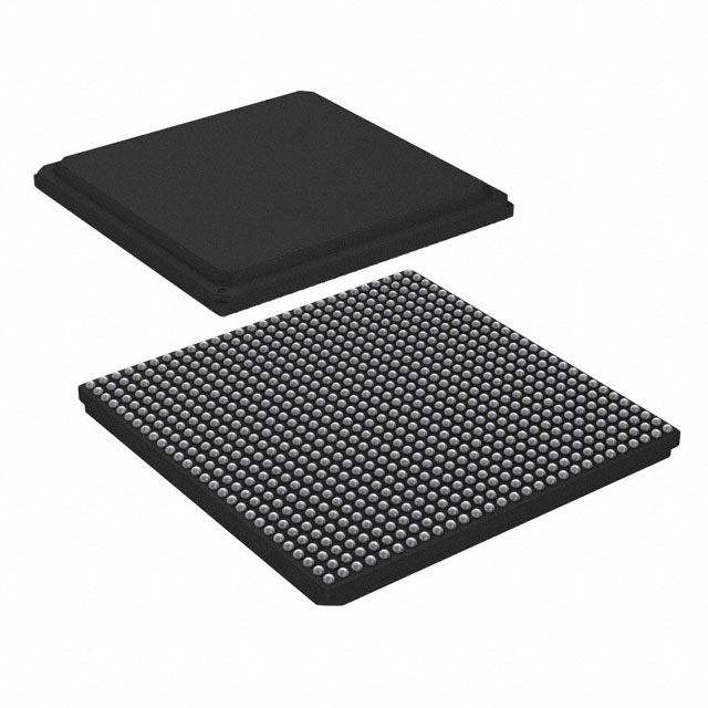
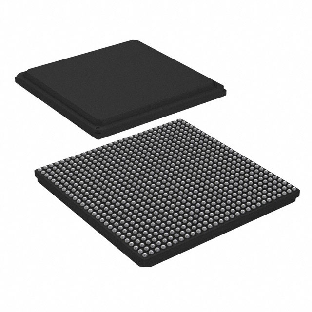
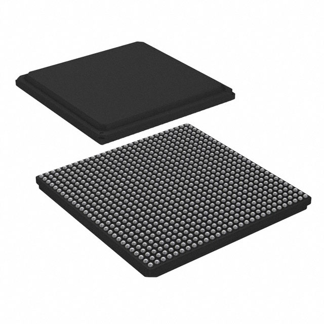
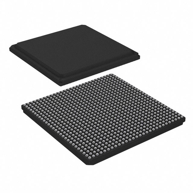
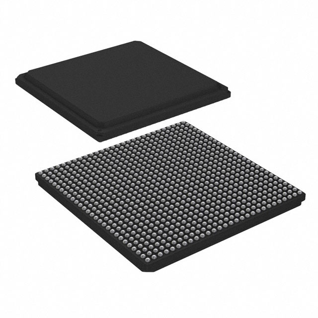
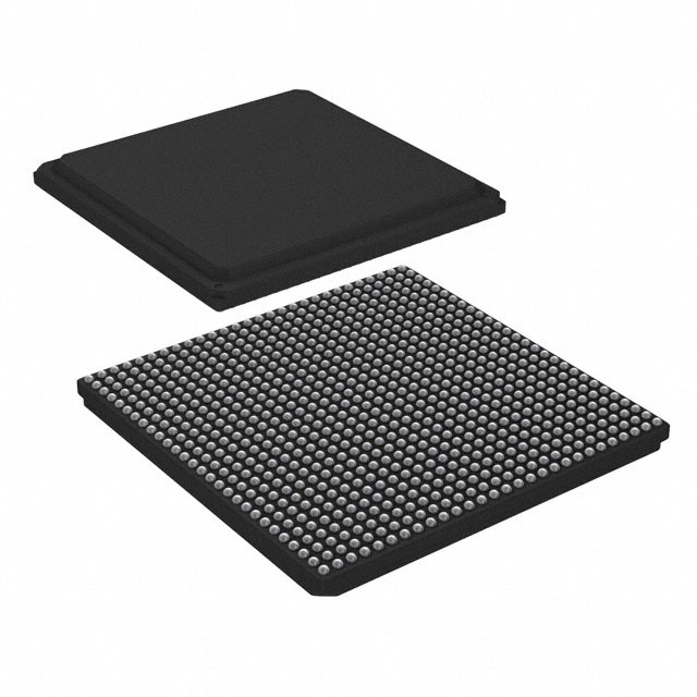
ARM® Cortex®-A72 Microprocessor IC QorIQ® Layerscape 2 Core, 64-Bit 1.2GHz 780-FCPBGA (23x23) |
|---|---|
| Quantity | 1,430 Available (as of October 8, 2026) |
| Product Category | Microprocessors |
|---|---|
| Part Series | LS1026A |
| Manufacturer | NXP USA Inc. |
| Manufacturing Status | Active |
| Manufacturer Standard Lead Time | 18 Weeks |
| Datasheet |
Specifications & Environmental
| Core Processor | ARM® Cortex®-A72 | Device Package | 780-FCPBGA (23x23) | ECCN | 5A002A1 NXP | ||
|---|---|---|---|---|---|---|---|
| Ethernet | 10GbE (2), 2.5GbE (1), 1GbE (4) | HTS Code | 8542.31.0001 | Moisture Sensitivity Level | 3 (168 Hours) | ||
| Mounting Method | Surface Mount | Mounting Type | Surface Mount | Number of Cores/Bus Width | 2 Core, 64-Bit | ||
| Operating Temperature | -40°C ~ 105°C | Package / Case | 780-FBGA, FCBGA | RAM Controllers | DDR4 | ||
| REACH Compliance | REACH Unaffected | RoHS Compliance | ROHS3 Compliant | SATA | SATA 6Gbps (1) | ||
| Security Features | Secure Boot, TrustZone® | Speed | 1.2GHz | Supplier Device Package | 780-FCPBGA (23×23) | ||
| USB | USB 3.0 (3) + PHY |
Overview of LS1026AXE8MQA – IC MPU QORIQ 1.2GHZ 780FCPBGA
The LS1026AXE8MQA is a dual-core, 64-bit ARM® Cortex®-A72 microprocessor in the NXP QorIQ Layerscape family, operating at 1.2 GHz. It combines high-performance CPU cores with integrated packet-processing acceleration and a broad set of high-speed interfaces for embedded networking, storage, security and industrial applications.
Designed for industrial qualification and wide temperature operation, the device targets designs demanding consolidated connectivity, hardware-assisted packet handling and on-chip security support while simplifying system integration through DDR4 memory support and a compact 23 × 23 mm FCPBGA package.
Key Features
- Core Dual ARM® Cortex®-A72 cores, 64-bit architecture at 1.2 GHz for compute-intensive embedded tasks.
- Memory Integrated DDR4 memory controller for modern high-bandwidth system memory.
- Networking Multiple integrated Ethernet controllers: two 10 GbE, one 2.5 GbE and four 1 GbE ports to support diverse network topologies and throughput requirements.
- Storage & USB SATA 6 Gbps interface for storage subsystems and three USB 3.0 ports with PHY for high-speed peripheral connectivity.
- High-speed I/O PCIe® Gen3 capability and high-speed SERDES connectivity (as described in series datasheet) for expansion and high-throughput I/O.
- Security Hardware-supported Secure Boot and ARM® TrustZone® for platform integrity and system-level isolation.
- Packaging & Mounting 780-FCPBGA package (23 × 23 mm), surface-mount with industrial-grade mounting and assembly compatibility.
- Operating Range & Compliance Industrial qualification with an operating temperature range of −40 °C to 105 °C and RoHS compliance.
Typical Applications
- Enterprise Routing & Switching Use the integrated multi-rate Ethernet and packet processing acceleration to implement control-plane and line-card controller functions.
- Network Attached Storage (NAS) Combine SATA 6 Gbps, high-speed PCIe I/O and USB 3.0 to deliver connected storage solutions with high throughput.
- Security Appliances Leverage Secure Boot, TrustZone and on-chip security acceleration for encrypted tunnels and secure gateway functions.
- Service Provider Gateways & vCPE Scale network functions with hardware acceleration and multiple Ethernet ports for managed CPE and gateway platforms.
- Single Board Computers Integrate into compact SBC designs requiring industrial temperature support and a rich set of peripherals.
Unique Advantages
- Integrated high-speed interfaces: Two 10 GbE, one 2.5 GbE, four 1 GbE, SATA 6 Gbps and multiple USB 3.0 ports reduce external PHY and bridge requirements.
- Hardware packet processing acceleration: On-chip packet handling offloads general-purpose cores to improve deterministic packet throughput and system efficiency.
- Built-in platform security: Secure Boot and ARM TrustZone support system integrity and trusted execution without adding external security controllers.
- Industrial-qualified temperature range: −40 °C to 105 °C supports deployment in harsh and wide-temperature environments.
- Compact BGA package: 780-FCPBGA (23 × 23 mm) balances high I/O density with a small PCB footprint for embedded system designs.
- DDR4 memory support: Modern memory interface for higher bandwidth and system performance in data- and packet-intensive applications.
Why Choose LS1026AXE8MQA?
The LS1026AXE8MQA delivers a balanced combination of dual ARM® Cortex®-A72 compute performance, multi-rate Ethernet connectivity and hardware packet acceleration in an industrial-grade package. Its integrated security features and modern memory interface make it suitable for embedded networking, storage and security-focused products that require consolidated functionality and reliable operation across wide temperatures.
Customers designing systems that demand high-speed interfaces, on-chip packet handling and industrial qualification will find the LS1026AXE8MQA a practical building block for scalable, maintainable platform designs within the Layerscape ecosystem.
Request a quote or submit a procurement inquiry to receive pricing and availability information for the LS1026AXE8MQA.



















Date Founded: 2006
Headquarters: Eindhoven, North Brabant, Netherlands
Employees: 38,000+
Revenue: $10.53 Billion
Certifications and Memberships: ISO9001:2015, IATF16949:2016


