
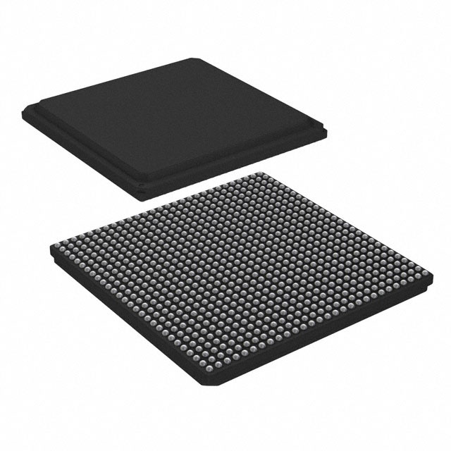
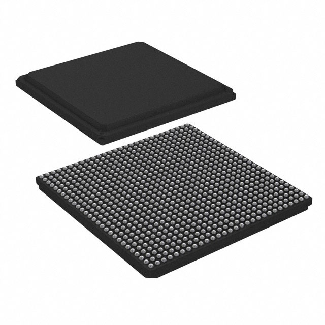
LS1026AXN8P1A
| Part Description |
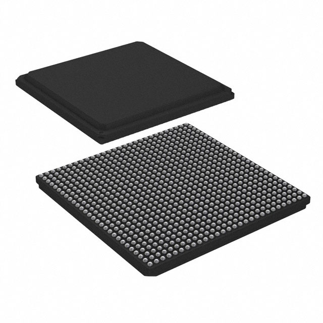
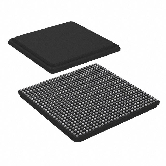
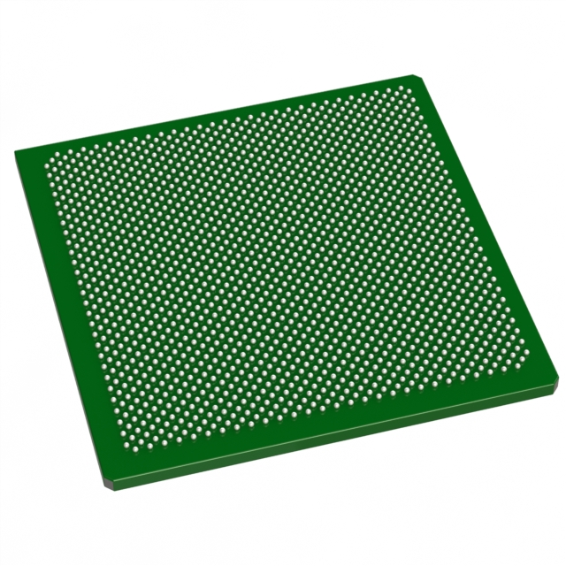
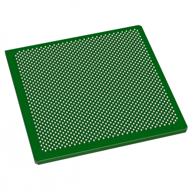
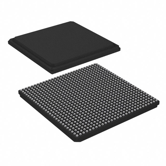
ARM® Cortex®-A72 Microprocessor IC QorIQ® Layerscape 2 Core, 64-Bit 1.4GHz 780-FCPBGA (23x23) |
|---|---|
| Quantity | 221 Available (as of October 8, 2026) |
| Product Category | Microprocessors |
|---|---|
| Part Series | LS1026A |
| Manufacturer | NXP USA Inc. |
| Manufacturing Status | Active |
| Manufacturer Standard Lead Time | 18 Weeks |
| Datasheet |
Specifications & Environmental
| Core Processor | ARM® Cortex®-A72 | Device Package | 780-FCPBGA (23x23) | ECCN | 5A002A1 NXP | ||
|---|---|---|---|---|---|---|---|
| Ethernet | 10GbE (2), 2.5GbE (1), 1GbE (4) | HTS Code | 8542.31.0001 | Moisture Sensitivity Level | 3 (168 Hours) | ||
| Mounting Method | Surface Mount | Mounting Type | Surface Mount | Number of Cores/Bus Width | 2 Core, 64-Bit | ||
| Operating Temperature | -40°C ~ 105°C | Package / Case | 780-FBGA, FCBGA | RAM Controllers | DDR4 | ||
| REACH Compliance | REACH Unaffected | RoHS Compliance | ROHS3 Compliant | SATA | SATA 6Gbps (1) | ||
| Security Features | Secure Boot, TrustZone® | Speed | 1.4GHz | Supplier Device Package | 780-FCPBGA (23×23) | ||
| USB | USB 3.0 (3) + PHY |
Overview of LS1026AXN8P1A – ARM Cortex‑A72 2‑Core 1.4 GHz MPU (780‑FCPBGA)
The LS1026AXN8P1A is an NXP QorIQ Layerscape microprocessor IC featuring two 64‑bit ARM® Cortex®‑A72 cores running at 1.4 GHz. It integrates high‑speed peripherals and packet processing elements targeted at networking, storage, security and industrial embedded designs.
Designed for enterprise and service‑provider applications, the device combines multi‑Gigabit Ethernet, USB 3.0, SATA and DDR4 memory support with on‑chip security and packet acceleration to deliver a compact, industrial‑rated processing building block.
Key Features
- Core Dual ARM® Cortex®‑A72 64‑bit cores running at 1.4 GHz, providing a balanced compute profile for control plane and application tasks.
- Memory Integrated DDR4 memory controller for modern system memory performance and bandwidth.
- Networking & High‑Speed I/O Multiple Ethernet controllers including two 10 GbE, one 2.5 GbE and four 1 GbE ports; includes high‑speed SerDes and PCIe Gen3 capability as part of the Layerscape family feature set.
- Storage & USB SATA 6 Gbps (SATA 3.0) interface for storage devices and three USB 3.0 ports with PHY for high‑speed host and device connectivity.
- Security & Acceleration Secure Boot and ARM TrustZone® are supported; the series integrates a security engine for high‑speed protocol processing and cryptographic offload.
- Packet Processing Acceleration On‑chip packet acceleration and hardware elements for parsing, classification, distribution, queue and buffer management to offload packet handling from application cores.
- Package & Temperature 780‑FCPBGA (23 × 23 mm) surface‑mount package with industrial operating range from −40 °C to 105 °C.
- Compliance RoHS‑compliant and qualified for industrial applications.
Typical Applications
- Enterprise Routers & Switches — Two 10 GbE ports, multi‑rate Ethernet and packet acceleration enable high‑performance control and data‑plane functions.
- Linecard Controllers — Integrated high‑speed I/O and packet processing help implement linecard control and traffic management tasks.
- Network Attached Storage (NAS) — SATA 6 Gbps plus USB 3.0 and DDR4 support enable NAS controller designs that require storage throughput and connectivity.
- Security Appliances — On‑chip security engine, Secure Boot and TrustZone® support accelerated protocol processing for IPsec/SSL/DTLS workloads.
- Single Board Computers & vCPE — Compact BGA package and rich I/O make the processor suitable for SBCs and virtual CPE platforms requiring industrial temperature operation.
Unique Advantages
- Highly integrated interfaces: Multiple 10 GbE/2.5 GbE/1 GbE ports, SATA and USB 3.0 reduce external PHY and bridge requirements for space‑constrained designs.
- Packet acceleration built in: Hardware parse, classify and buffer management offload routine packet tasks from the cores, improving application efficiency.
- Security architecture: Secure Boot and ARM TrustZone®, together with an integrated security engine, enable protected boot and accelerated crypto for secure deployments.
- Industrial temperature rating: −40 °C to 105 °C qualification supports deployment in harsh and industrial environments.
- Family scalability: Pin and software compatibility across the Layerscape LS10xx family enables hardware and software reuse for design scaling.
- Compact package: 780‑FCPBGA (23 × 23 mm) surface‑mount package balances density and thermal considerations for embedded modules and SBCs.
Why Choose LS1026AXN8P1A?
The LS1026AXN8P1A combines dual ARM Cortex‑A72 processing with integrated DDR4, multi‑rate Ethernet, SATA and USB 3.0 interfaces, plus on‑chip packet and security acceleration to deliver a capable, compact MPU for networking, storage and security applications. Its industrial temperature rating and RoHS compliance make it suitable for demanding embedded deployments.
Choose this device when you need a scalable Layerscape solution that supports hardware/software compatibility across the family, simplifies board‑level integration and accelerates time‑to‑market for enterprise and service provider designs.
Request a quote or submit an inquiry to get pricing and availability for LS1026AXN8P1A.



















Date Founded: 2006
Headquarters: Eindhoven, North Brabant, Netherlands
Employees: 38,000+
Revenue: $10.53 Billion
Certifications and Memberships: ISO9001:2015, IATF16949:2016


