
MC68360AI25VL
| Part Description |
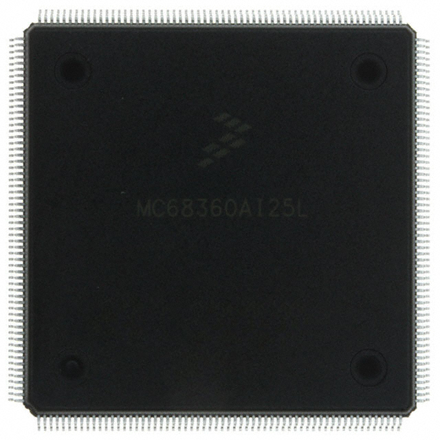
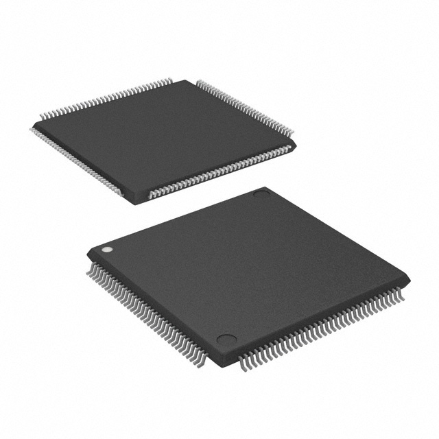
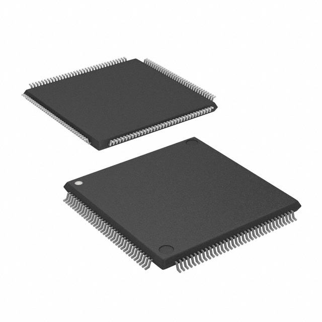
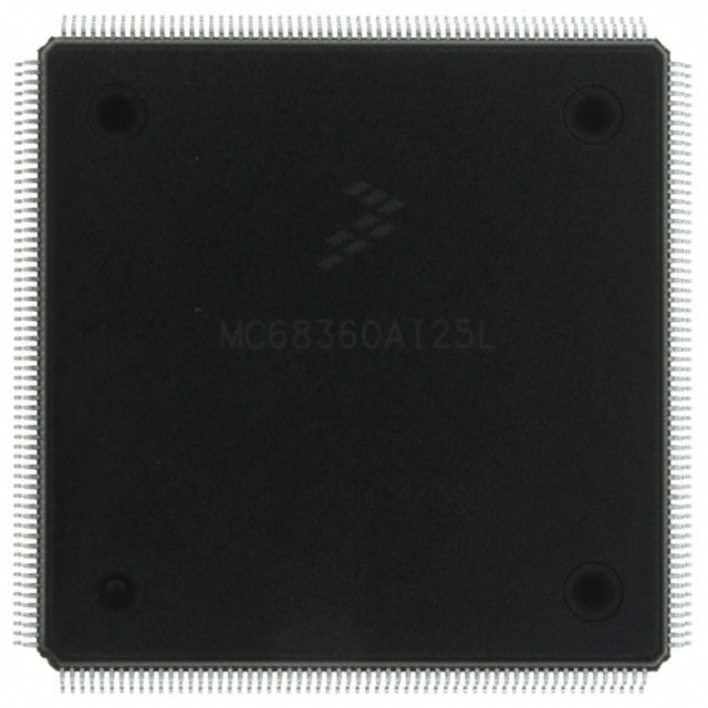
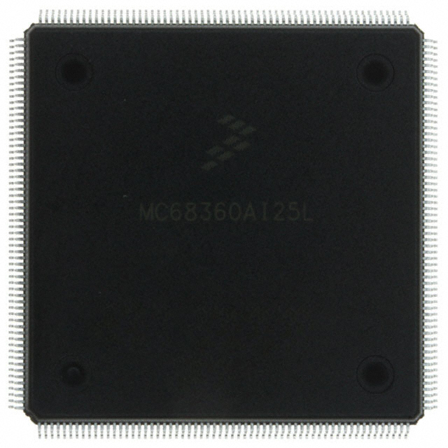
CPU32+ Microprocessor IC M683xx 1 Core, 32-Bit 25MHz 240-FQFP (32x32) |
|---|---|
| Quantity | 313 Available (as of October 8, 2026) |
| Product Category | Microprocessors |
|---|---|
| Part Series | MC68360 |
| Manufacturer | NXP USA Inc. |
| Manufacturing Status | Obsolete |
| Manufacturer Standard Lead Time | Contact Us |
| Datasheet |
Specifications & Environmental
| Co-Processors/DSP | Communications; CPM | Core Processor | CPU32+ | Device Package | 240-FQFP (32x32) | ||
|---|---|---|---|---|---|---|---|
| ECCN | 3A991A2 | Ethernet | 10Mbps (1) | Graphics Acceleration | No | ||
| HTS Code | 8542.31.0001 | Moisture Sensitivity Level | 3 (168 Hours) | Mounting Method | Surface Mount | ||
| Mounting Type | Surface Mount | Number of Cores/Bus Width | 1 Core, 32-Bit | Operating Temperature | 0°C ~ 70°C (TA) | ||
| Package / Case | 240-BFQFP | RAM Controllers | DRAM | REACH Compliance | REACH Unaffected | ||
| RoHS Compliance | ROHS3 Compliant | Speed | 25MHz | Supplier Device Package | 240-FQFP (32×32) | ||
| Voltage – I/O | 3.3V |
Overview of MC68360AI25VL – IC MPU M683XX 25MHZ 240FQFP
The MC68360AI25VL is a CPU32+ microprocessor from the MC68360 QUICC family, implemented as a single 32-bit core running at 25 MHz in a 240-pin FQFP surface-mount package. It combines a CPU32+ core with an integrated communications processor module (CPM) and a broad set of on-chip peripherals targeted at communications and embedded controller applications.
Designed for controller and communications roles, the device integrates memory control, multiple serial channels, DMA, timers and a system integration module to simplify system design and reduce external component count while supporting standard 3.3 V I/O and commercial temperature operation.
Key Features
- Core — CPU32+ single 32-bit core operating at 25 MHz; complete static design supporting 0–33 MHz operation as described in the device family documentation.
- Memory — On-chip memory controller with support for DRAM (eight-bank controller) and glueless interfaces to common memory types; boot chip select available at reset with options for 8-, 16- or 32-bit memory widths.
- Communications Co-processor (CPM) — Integrated CPM for communications handling and offloading protocol tasks from the CPU core.
- Serial Interfaces — Multiple serial channels including four Serial Communications Controllers (SCCs), two Serial Management Controllers (SMCs) and one Serial Peripheral Interface (SPI) for diverse serial connectivity.
- Ethernet — Integrated 10 Mbps Ethernet interface (1 port) for basic network connectivity.
- Timers & DMA — Four general-purpose timers (configurable as four 16-bit or two 32-bit timers) and two independent DMA channels (IDMAs) for deterministic data movement and timing.
- System Integration — System Integration Module (SIM60) with bus monitor, breakpoint logic, periodic interrupt timer, on-chip bus arbitration and support for external masters and companion-mode operation.
- Package & Mounting — 240-lead Plastic Quad Flat Pack (240-FQFP, 32×32 mm footprint) intended for surface-mount assembly.
- Power & I/O — 3.3 V I/O supply level as specified in product data.
- Operating Range — Commercial temperature range: 0°C to 70°C.
- Compliance — RoHS compliant.
Typical Applications
- ISDN and Telecom Equipment — On-chip CPM, multiple serial channels and integrated timers make the device suitable for telephony and telecom controller functions.
- Mid-range Routers and LAN Switches — Integrated serial interfaces, DMA and an Ethernet port support packet handling and peripheral control in network equipment.
- Bridges and Network Gateways — The combination of CPU core, communications processors and memory controller enables protocol handling and buffering for gateway applications.
- Wireless Infrastructure — Communications-focused peripheral set and system integration features support base station and infrastructure controller tasks.
Unique Advantages
- Integrated communications peripherals: Four SCCs, two SMCs and SPI plus a CPM reduce external interface chips and simplify communications stack integration.
- Single-chip system controller: On-chip CPU, memory controller, timers, DMA and SIM60 lower BOM count and streamline PCB design.
- Flexible memory support: Eight-bank DRAM controller and glueless interfaces to common memory types provide versatile system memory options and boot-time configuration.
- Deterministic I/O and data movement: Dedicated IDMAs and multiple timers enable predictable data transfer and timing for embedded control tasks.
- Commercial temperature and surface-mount packaging: 240-FQFP surface-mount package and 0°C to 70°C operation match common industrial and communications product requirements.
- RoHS compliant: Facilitates use in modern assemblies requiring lead-free components.
Why Choose MC68360AI25VL?
The MC68360AI25VL positions itself as a communications-focused single-chip microprocessor that brings together a CPU32+ core and a rich set of on-chip peripherals—memory controller, CPM, multiple serial channels, DMA and timers—into a 240-FQFP surface-mount package. This integration reduces board-level complexity and supports designs where integrated communications handling and deterministic I/O are important.
This part is suited to engineers designing mid-range networking, telecom and embedded communications controllers who require a 32-bit CPU at 25 MHz with dedicated communications resources, flexible memory interfacing and standard 3.3 V I/O. Its RoHS compliance and commercial temperature range support production deployments in typical embedded and communications equipment.
Request a quote or submit an inquiry to receive pricing and availability information for MC68360AI25VL.






















Date Founded: 2006
Headquarters: Eindhoven, North Brabant, Netherlands
Employees: 38,000+
Revenue: $10.53 Billion
Certifications and Memberships: ISO9001:2015, IATF16949:2016


