
MCIMX355AJQ5C
| Part Description |
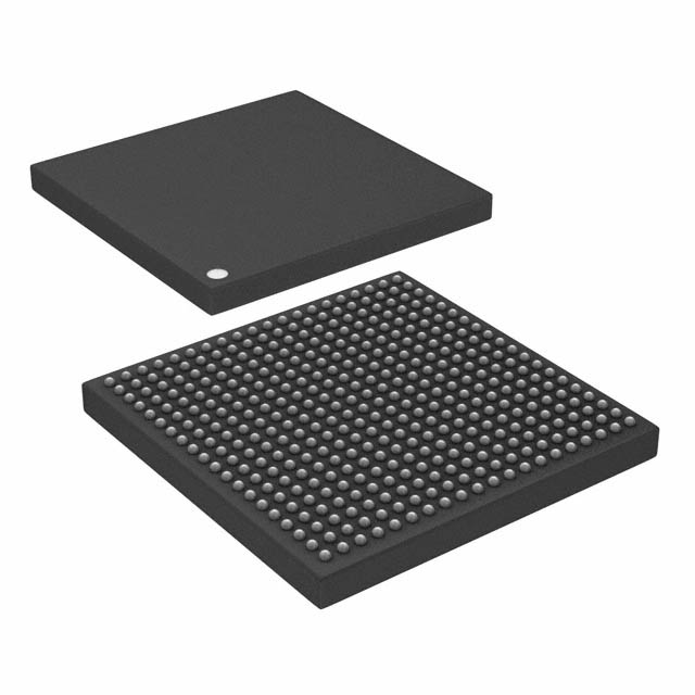
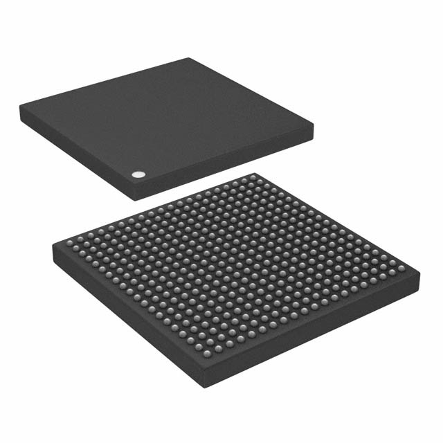
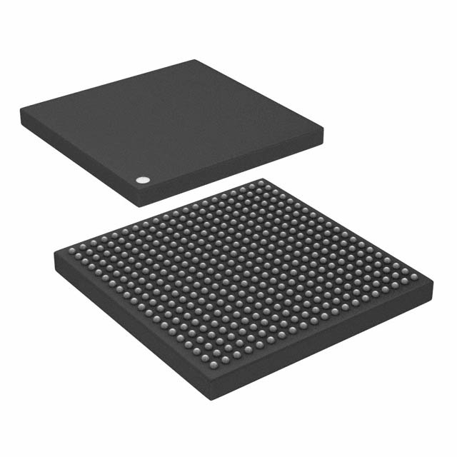
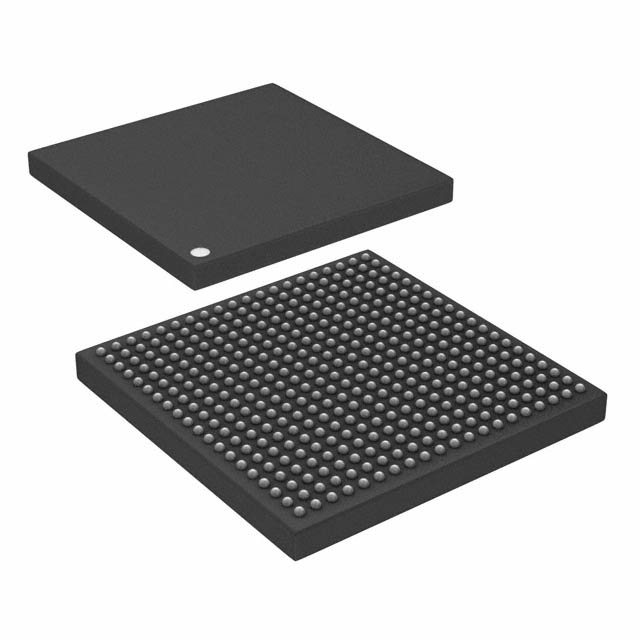
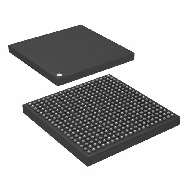
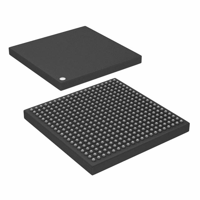
ARM1136JF-S Microprocessor IC i.MX35 1 Core, 32-Bit 532MHz 400-LFBGA (17x17) |
|---|---|
| Quantity | 941 Available (as of October 8, 2026) |
| Product Category | Microprocessors |
|---|---|
| Part Series | i.MX 355 |
| Manufacturer | NXP USA Inc. |
| Manufacturing Status | Active |
| Manufacturer Standard Lead Time | 13 Weeks |
| Datasheet |
Specifications & Environmental
| Co-Processors/DSP | Multimedia; IPU, VFP | Core Processor | ARM1136JF-S | Device Package | 400-LFBGA (17x17) | ||
|---|---|---|---|---|---|---|---|
| Display & Interface Controllers | Keypad, KPP, LCD | ECCN | 5A992C | Ethernet | 10/100Mbps (1) | ||
| Graphics Acceleration | No | HTS Code | 8542.31.0001 | Moisture Sensitivity Level | 3 (168 Hours) | ||
| Mounting Method | Surface Mount | Mounting Type | Surface Mount | Number of Cores/Bus Width | 1 Core, 32-Bit | ||
| Operating Temperature | -40°C ~ 85°C (TA) | Package / Case | 400-LFBGA | RAM Controllers | LPDDR, DDR2 | ||
| REACH Compliance | REACH Unaffected | RoHS Compliance | ROHS3 Compliant | Security Features | Secure Fusebox, Secure JTAG | ||
| Speed | 532MHz | Supplier Device Package | 400-LFBGA (17×17) | USB | USB 2.0 + PHY (2) | ||
| Voltage – I/O | 1.8V, 2.0V, 2.5V, 2.7V, 3.0V, 3.3V |
Overview of MCIMX355AJQ5C – IC MPU I.MX35 532MHZ 400LFBGA
The MCIMX355AJQ5C is an embedded microprocessor based on the ARM1136JF-S core, delivering a single 32‑bit core operating at 532 MHz. Designed for industrial embedded applications, the device integrates a broad set of system interfaces and memory controllers to simplify system design and accelerate product development.
Key value comes from its on‑chip connectivity and system integration—dual USB 2.0 with PHY, 10/100 Mbps Ethernet, LPDDR/DDR2 memory controllers and built‑in security features—packaged in a 400‑LFBGA (17×17 mm) surface‑mount package rated for industrial temperature ranges.
Key Features
- Core ARM1136JF‑S single 32‑bit core running at 532 MHz for deterministic embedded processing.
- Memory Controllers Integrated memory controllers supporting LPDDR and DDR2 to interface with common off‑chip DRAM options.
- Interfaces Dual USB 2.0 controllers with PHY, single 10/100 Mbps Ethernet port and an additional 1‑Wire interface for peripheral connectivity.
- Display & Input On‑chip display interface controllers including LCD and keypad (KPP) support for human‑machine interfaces.
- Co‑processors Multimedia offload with IPU and VFP to accelerate specific signal and media processing tasks.
- Security Secure Fusebox and Secure JTAG features for device provisioning and secure debug/control.
- Package & Mounting 400‑LFBGA package in a 17×17 mm footprint, surface‑mount mounting for compact board designs.
- Operating Range Industrial qualification with an operating temperature range of −40 °C to 85 °C and RoHS compliance for regulatory alignment.
- Graphics No dedicated graphics acceleration, simplifying selection where GPU offload is not required.
Typical Applications
- Industrial Embedded Systems Control and monitoring systems that require a compact, industrial‑rated processor with Ethernet and USB connectivity.
- Human‑Machine Interfaces (HMI) LCD and keypad support make the device suitable for operator panels and interface controllers.
- Multimedia Control Devices Processors for audio and media control appliances that leverage the multimedia co‑processors and VFP support.
- Connectivity Gateways Embedded gateway devices using onboard USB and 10/100 Mbps Ethernet for peripheral and network interfacing.
Unique Advantages
- Integrated System Interfaces: Dual USB 2.0 with PHY and 10/100 Ethernet reduce external component count and simplify board-level design.
- Flexible Memory Support: On‑chip LPDDR and DDR2 controllers enable designers to choose DRAM options that match performance and cost targets.
- Industrial Temperature Rating: −40 °C to 85 °C operation supports deployment in harsh or temperature‑variable environments.
- Security Primitives On‑Chip: Secure Fusebox and Secure JTAG provide hardware-level mechanisms for secure provisioning and debugging.
- Compact, Surface‑Mount Package: 400‑LFBGA (17×17 mm) allows dense layouts and compact end‑product designs.
- Standards‑Aligned Compliance: RoHS compliance supports regulatory and environmental requirements during manufacturing.
Why Choose MCIMX355AJQ5C?
The MCIMX355AJQ5C positions itself as a compact, industrial‑rated embedded processor that balances single‑core ARM performance with a broad set of integrated interfaces and security features. It is well suited to designers who need deterministic processing at 532 MHz, built‑in connectivity (USB, Ethernet), and flexible DRAM support in a small surface‑mount package.
Backed by NXP Semiconductors manufacturing, this part is appropriate for embedded product lines where system integration, industrial temperature operation, and hardware security primitives are required for long‑term, reliable deployments.
Request a quote or submit an inquiry for MCIMX355AJQ5C to get pricing, availability, and assistance in qualifying this device for your next embedded design.





















Date Founded: 2006
Headquarters: Eindhoven, North Brabant, Netherlands
Employees: 38,000+
Revenue: $10.53 Billion
Certifications and Memberships: ISO9001:2015, IATF16949:2016


