
MCIMX355AVM5BR2
| Part Description |
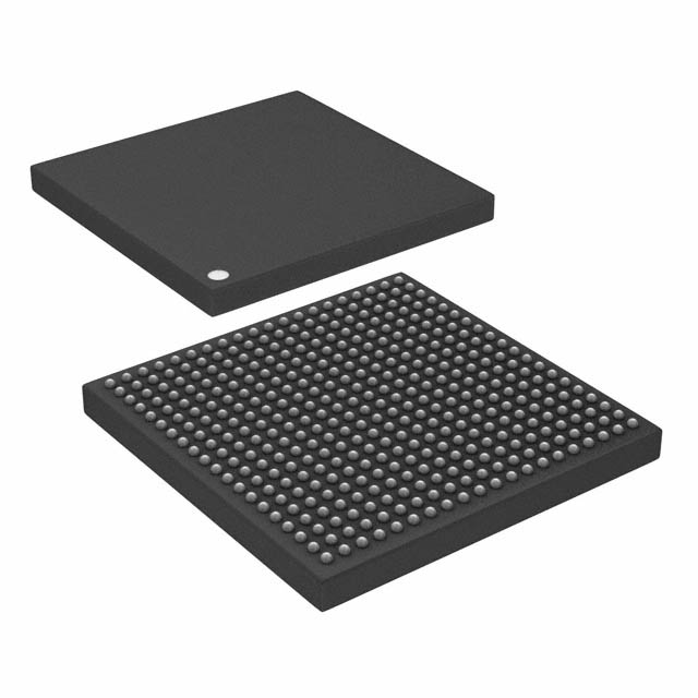
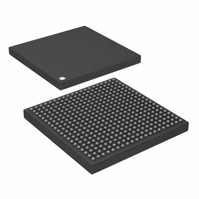
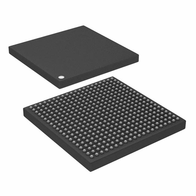
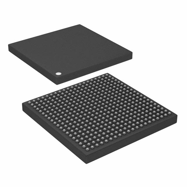
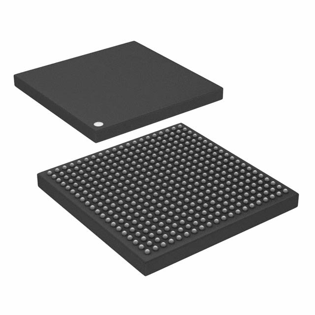
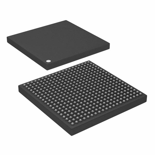
ARM1136JF-S Microprocessor IC i.MX35 1 Core, 32-Bit 532MHz 400-LFBGA (17x17) |
|---|---|
| Quantity | 1,295 Available (as of October 8, 2026) |
| Product Category | Microprocessors |
|---|---|
| Part Series | i.MX 355 |
| Manufacturer | NXP USA Inc. |
| Manufacturing Status | Active |
| Manufacturer Standard Lead Time | 13 Weeks |
| Datasheet |
Specifications & Environmental
| Co-Processors/DSP | Multimedia; IPU, VFP | Core Processor | ARM1136JF-S | Device Package | 400-LFBGA (17x17) | ||
|---|---|---|---|---|---|---|---|
| Display & Interface Controllers | Keypad, KPP, LCD | ECCN | 5A992C | Ethernet | 10/100Mbps (1) | ||
| Graphics Acceleration | No | HTS Code | 8542.31.0001 | Moisture Sensitivity Level | 3 (168 Hours) | ||
| Mounting Method | Surface Mount | Mounting Type | Surface Mount | Number of Cores/Bus Width | 1 Core, 32-Bit | ||
| Operating Temperature | -40°C ~ 85°C (TA) | Package / Case | 400-LFBGA | RAM Controllers | LPDDR, DDR2 | ||
| REACH Compliance | REACH Unaffected | RoHS Compliance | ROHS3 Compliant | Security Features | Secure Fusebox, Secure JTAG | ||
| Speed | 532MHz | Supplier Device Package | 400-LFBGA (17×17) | USB | USB 2.0 + PHY (2) | ||
| Voltage – I/O | 1.8V, 2.0V, 2.5V, 2.7V, 3.0V, 3.3V |
Overview of MCIMX355AVM5BR2 – IC MPU I.MX35 532MHZ 400LFBGA
The MCIMX355AVM5BR2 is an NXP Semiconductors microprocessor based on the ARM1136JF-S core. It is a single‑core, 32‑bit application processor running at up to 532 MHz and targets embedded designs that require integrated multimedia, connectivity and control functions.
Designed for automotive infotainment, navigation and A/V/telematics use cases at the series level, the device combines multimedia co‑processors, multiple peripheral controllers and broad memory support to deliver a compact, automotive‑oriented processing solution with wide operating temperature capability.
Key Features
- Core & Performance — ARM1136JF‑S single 32‑bit core running up to 532 MHz, providing a balance of compute for embedded multimedia and control tasks.
- Multimedia Co‑processors — Integrated multimedia engines including IPU and VFP to support audio and video processing functions referenced in the series documentation.
- Memory Support — Built‑in memory controllers for LPDDR and DDR2 devices, simplifying external memory interfacing for system designs.
- Display & User Interface — On‑chip display interface controllers including keypad/KPP and LCD support for graphical user interfaces and control panels.
- Connectivity — Single 10/100 Mbps Ethernet controller and two USB 2.0 ports with PHY provide wired network and host/device connectivity options.
- Peripheral Interfaces — Additional interfaces such as 1‑Wire expand peripheral and accessory connectivity.
- Security — Secure Fusebox and Secure JTAG features for hardware-level security and controlled debug access.
- Automotive Qualification (series‑level) — Series documentation indicates AEC‑Q100 Grade 3 qualification for automotive applications (series‑level reference).
- Package & Temperature — 400‑LFBGA package in a 17 × 17 mm footprint with 0.8 mm pitch and an operating temperature range of −40 °C to 85 °C.
- Compliance — RoHS compliant.
Typical Applications
- Automotive Infotainment Systems — Drives audio playback, user interfaces and media management in vehicle infotainment platforms as described in the series documentation.
- Navigation & Map Display — Supports map display and route calculation tasks with dedicated display controllers and multimedia resources.
- Telematics & Audio Connectivity — Enables hands‑free telephony, audio connectivity and telematics functions with integrated audio processing and USB connectivity.
- In‑vehicle Multimedia Interfaces — Suitable for QVGA/WVGA display support and GUI implementations referenced in the series materials.
Unique Advantages
- Highly integrated feature set: Multimedia co‑processors, display controllers, Ethernet and dual USB 2.0 with PHY reduce external component count and simplify system design.
- Automotive‑oriented documentation and qualification: Series‑level AEC‑Q100 Grade 3 qualification and automotive application focus support vehicle electronics use cases.
- Security primitives on‑chip: Secure Fusebox and Secure JTAG provide hardware mechanisms to protect firmware and control debug access.
- Flexible memory interfacing: Native LPDDR and DDR2 controllers allow designers to choose memory configurations that match performance and cost targets.
- Wide operating range and compact package: −40 °C to 85 °C operation in a 17 × 17 mm 400‑LFBGA package enables deployment in temperature‑challenging embedded environments.
Why Choose MCIMX355AVM5BR2?
The MCIMX355AVM5BR2 positions itself as a compact, automotive‑focused application processor combining an ARM1136JF‑S core at 532 MHz with integrated multimedia co‑processors, diverse connectivity and memory interfaces. Its feature set supports common infotainment, navigation and telematics functions while simplifying BOM and board design through on‑chip peripherals.
Ideal for embedded system designers targeting vehicle A/V and navigation platforms, this part offers a balance of processing capability, integrated interfaces and series‑level automotive qualification, backed by NXP Semiconductors product documentation and support resources.
Request a quote or submit an inquiry to receive pricing and availability information for the MCIMX355AVM5BR2.





















Date Founded: 2006
Headquarters: Eindhoven, North Brabant, Netherlands
Employees: 38,000+
Revenue: $10.53 Billion
Certifications and Memberships: ISO9001:2015, IATF16949:2016


