
10AT115U4F45E3SGES
| Part Description |
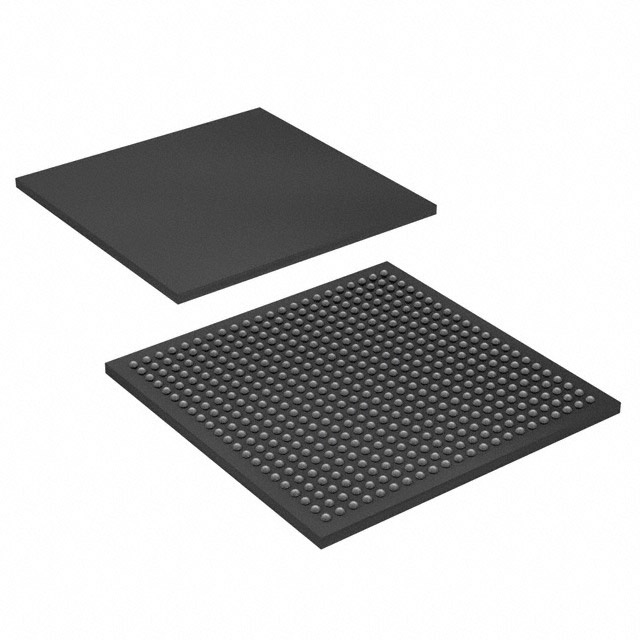
Arria 10 GT Field Programmable Gate Array (FPGA) IC 624 68857856 1150000 1932-BBGA, FCBGA |
|---|---|
| Quantity | 690 Available (as of June 15, 2026) |

| Product Category | Field Programmable Gate Array (FPGA) |
|---|---|
| Manufacturer | Intel |
| Manufacturing Status | Obsolete |
| Manufacturer Standard Lead Time | Contact Us |
| Datasheet |
Specifications & Environmental
| Device Package | 1932-FBGA, FC (45x45) | Grade | Extended | Operating Temperature | 0°C – 100°C | ||
|---|---|---|---|---|---|---|---|
| Package / Case | 1932-BBGA, FCBGA | Number of I/O | 624 | Voltage | 870 mV - 930 mV | ||
| Mounting Method | Surface Mount | RoHS Compliance | Unknown | REACH Compliance | REACH Unaffected | ||
| Moisture Sensitivity Level | 3 (168 Hours) | Number of LABs/CLBs | 427200 | Number of Logic Elements/Cells | 1150000 | ||
| Number of Gates | N/A | ECCN | 3A001A7A | HTS Code | 8542.39.0001 | ||
| Qualification | N/A | Total RAM Bits | 68857856 |
Overview of 10AT115U4F45E3SGES – Arria 10 GT FPGA, 1932-BBGA (1,150,000 logic elements)
The 10AT115U4F45E3SGES is an Intel Arria 10 GT Field Programmable Gate Array (FPGA) optimized for mid-range, high-performance and power-sensitive applications. It is a 20 nm-class device variant in the Arria 10 family, combining a high logic capacity with embedded memory and serial transceiver capabilities suitable for demanding communications and compute tasks.
Targeted markets include wireless, wireline, broadcast, computing and storage, medical, and military communications. The device’s combination of high logic density, substantial on-chip RAM and large I/O count delivers integration and system-level efficiency for complex designs.
Key Features
- Core Logic 1,150,000 logic elements provide high-density programmable logic for large-scale designs and complex algorithms.
- Embedded Memory 68,857,856 total RAM bits for on-chip buffering, lookup tables and data storage to reduce external memory dependence.
- I/O and Transceivers 624 I/O pins and Arria 10 GT’s low-power serial transceiver architecture enable high-bandwidth external interfaces and flexible connectivity options.
- DSP and Processing Blocks Variable-precision DSP block architecture (family-level) supports custom numeric precision for signal processing workloads.
- Hard IP and Interfaces Includes family-level hard IP support such as PCIe Gen1/Gen2/Gen3 and enhanced PCS hard IP for Interlaken and 10 Gbps Ethernet.
- Reconfiguration and Reliability Supports dynamic and partial reconfiguration and includes SEU error detection and correction features (family-level) to help maintain system reliability.
- Package and Mounting 1932-BBGA (FCBGA) package, supplier package 1932-FBGA FC (45×45), surface mount for compact, high-density board designs.
- Power and Thermal Nominal voltage supply range 870 mV to 930 mV; operating temperature 0 °C to 100 °C; Extended grade for broader deployment environments.
- Compliance RoHS compliant.
Typical Applications
- Wireless infrastructure Channel and switch cards in remote radio heads and mobile backhaul systems, leveraging high logic density and transceivers for radio and baseband processing.
- Wireline communications 40G/100G muxponders, transponders and line cards where integrated packet processing, hard IP and high-speed serial links are required.
- Broadcast and professional AV Studio switches and transport equipment that benefit from embedded memory and flexible I/O for video switching and buffering.
- Computing and storage Server acceleration, flash cache and cloud infrastructure applications that use on-chip logic and memory for acceleration and data-path processing.
- Medical and defense systems Diagnostic imaging, radar and secure communications applications that require deterministic logic and on-device memory.
Unique Advantages
- High logic capacity: 1,150,000 logic elements allow consolidation of multiple functions into a single device, reducing board-level complexity and BOM count.
- Large on-chip memory: 68.9 Mbits of embedded RAM supports heavy buffering and local data processing, lowering external memory needs and improving throughput.
- Extensive I/O and serial capability: 624 I/Os combined with Arria 10 GT transceiver architecture enables flexible, high-bandwidth interfaces to external devices and links.
- Integrated interface IP: Built-in support for PCIe Gen1/2/3 and enhanced PCS for Interlaken and 10 Gbps Ethernet speeds accelerates time-to-market for networking and compute designs.
- Flexible reconfiguration: Dynamic and partial reconfiguration support lets you update or partition functionality without full device reprogramming, enabling adaptive designs.
- Extended-grade and RoHS compliant: Operating range of 0 °C to 100 °C and RoHS compliance make the device suitable for a wide set of commercial and industrial applications.
Why Choose 10AT115U4F45E3SGES?
The 10AT115U4F45E3SGES positions itself as a high-density, mid-range FPGA option within the Intel Arria 10 family that balances performance and power efficiency. Its combination of more than one million logic elements, tens of megabits of embedded RAM, broad I/O and transceiver support, and family-level hard IP options make it well suited for communications, compute acceleration and other complex embedded systems.
Engineers building systems that demand integration, scalable logic resources and reliable on-chip memory will find this device aligns with long-term platform needs. Backed by the Arria 10 device documentation and ecosystem, it supports iterative development and deployment across a range of markets.
Request a quote or submit a technical inquiry to check pricing, availability and lead times for 10AT115U4F45E3SGES.


Date Founded: 1968
Headquarters: Santa Clara, California, USA
Employees: 130,000+
Revenue: $54.23 Billion
Certifications and Memberships: ISO9001:2015, ISO14001:2015, ISO17025:2017, ISO27001:2022, ISO45001:2018, ISO50001:2018


