
10AX027H2F35E1SG
| Part Description |
Arria 10 GX Field Programmable Gate Array (FPGA) IC 384 17870848 270000 1152-BBGA, FCBGA |
|---|---|
| Quantity | 14 Available (as of June 14, 2026) |

| Product Category | Field Programmable Gate Array (FPGA) |
|---|---|
| Manufacturer | Intel |
| Manufacturing Status | Discontinued |
| Manufacturer Standard Lead Time | 13 Weeks |
| Datasheet |
Specifications & Environmental
| Device Package | 1152-FCBGA (35x35) | Grade | Extended | Operating Temperature | 0°C – 100°C | ||
|---|---|---|---|---|---|---|---|
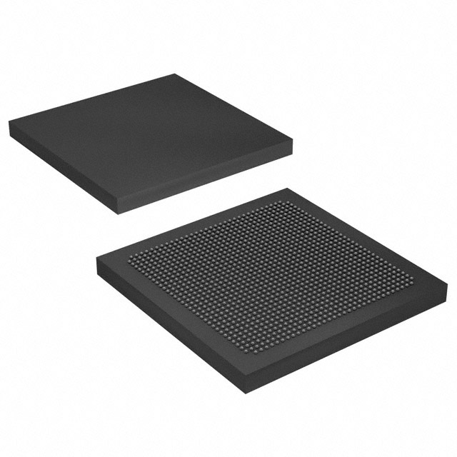
| Package / Case | 1152-BBGA, FCBGA | Number of I/O | 384 | Voltage | 870 mV - 980 mV | ||
| Mounting Method | Surface Mount | RoHS Compliance | RoHS Compliant | REACH Compliance | REACH Unaffected | ||
| Moisture Sensitivity Level | 3 (168 Hours) | Number of LABs/CLBs | 101620 | Number of Logic Elements/Cells | 270000 | ||
| Number of Gates | N/A | ECCN | 5A002A1 | HTS Code | 8542.39.0001 | ||
| Qualification | N/A | Total RAM Bits | 17870848 |
Overview of 10AX027H2F35E1SG – Arria 10 GX FPGA, 270,000 Logic Elements, 1152‑FCBGA
The 10AX027H2F35E1SG is an Intel Arria 10 GX Field Programmable Gate Array (FPGA) IC in a 1152‑FCPGA (35×35) package. Built on the Arria 10 device family architecture, it provides a mid‑range, 20‑nm FPGA platform optimized for high performance and power efficiency.
Targeted markets include wireless, wireline, broadcast, computing and storage, medical, and military applications. Key value propositions are high logic density, substantial on‑chip RAM, broad I/O capability, and features drawn from the Arria 10 architecture such as advanced DSP and reconfiguration support.
Key Features
- Core Logic — 270,000 logic elements to implement complex custom logic, control paths, and packet processing engines.
- Logic Structure — 101,620 logic blocks reported in device data for partitioning and synthesis planning.
- On‑Chip Memory — 17,870,848 total RAM bits to support buffering, caches, and in‑FPGA data storage for high‑bandwidth applications.
- I/O and Package — 384 user I/Os in a 1152‑FCBGA (35×35) surface‑mount package, enabling dense board routing and high pin count connectivity.
- Power and Thermal — Supported supply voltage range of 870 mV to 980 mV and operating temperature range of 0 °C to 100 °C; device is graded as Extended.
- Fabric and DSP — Arria 10 architecture includes adaptive logic modules and variable‑precision DSP blocks for custom arithmetic and signal‑processing implementations.
- Clocking and Reconfiguration — Rich clock networks, PLL clock sources, and support for dynamic and partial reconfiguration for runtime flexibility.
- High‑Speed Interfaces and IP — Arria 10 family features include low‑power serial transceivers, enhanced PCS hard IP for protocols like 10 Gbps Ethernet and Interlaken, and PCIe Gen1/2/3 hard IP.
- Standards and Compliance — RoHS compliant.
Typical Applications
- Wireless Infrastructure — Channel and switch cards in remote radio heads and mobile backhaul systems benefiting from high logic density and DSP capabilities.
- High‑Speed Wireline — Line cards, muxponders, and transponders (40G/100G) leveraging the device’s high‑speed transceivers and protocol hard IP.
- Broadcast and Media — Studio switches, transport, and professional audio/video processing that use on‑chip RAM and DSP blocks for buffering and real‑time processing.
- Computing and Storage Acceleration — Server acceleration, flash cache, and cloud compute offload where large logic resources and embedded memory support custom accelerators.
- Medical and Defense Systems — Diagnostic imaging, radar, and electronic warfare applications that require mid‑range FPGA performance with extended operating grade.
Unique Advantages
- High Logic Density: 270,000 logic elements enable implementation of large custom hardware functions and complex control logic on a single device.
- Substantial Embedded Memory: Nearly 18 Mbits of on‑chip RAM reduce external memory dependency for buffering and accelerate data‑intensive tasks.
- Comprehensive I/O and Packaging: 384 I/Os in a 1152‑FCBGA (35×35) package provide the pin count and physical footprint for dense system designs.
- Advanced Fabric Capabilities: Adaptive logic modules and variable‑precision DSP blocks support high‑throughput signal processing and arithmetic accelerators.
- Flexible System Integration: Clock network features, PLLs, dynamic/partial reconfiguration, and built‑in protocol hard IP simplify integration of networking and compute subsystems.
- Power‑Efficient 20‑nm Architecture: Arria 10 family design emphasizes power efficiency, supporting dense implementations with lower power budgets.
Why Choose 10AX027H2F35E1SG?
The 10AX027H2F35E1SG Arria 10 GX FPGA delivers a balance of high logic capacity, significant embedded RAM, and robust I/O in a 1152‑FCBGA package—making it suitable for mid‑range, performance‑sensitive applications across communications, broadcast, compute acceleration, medical, and defense markets. Its support for advanced DSP, flexible clocking, and high‑speed protocol IP stems directly from the Arria 10 device family architecture.
For designs that require scalable logic, on‑chip memory, and integrated interface capabilities with extended operating grade, this device provides a platform that aligns with professional engineering requirements while leveraging the Arria 10 feature set for long‑term design scalability.
Request a quote or submit an inquiry for pricing and availability to evaluate 10AX027H2F35E1SG for your next design.


Date Founded: 1968
Headquarters: Santa Clara, California, USA
Employees: 130,000+
Revenue: $54.23 Billion
Certifications and Memberships: ISO9001:2015, ISO14001:2015, ISO17025:2017, ISO27001:2022, ISO45001:2018, ISO50001:2018


