
10AX048K4F35I3LG
| Part Description |
Arria 10 GX Field Programmable Gate Array (FPGA) IC 396 5664768 480000 1152-BBGA, FCBGA |
|---|---|
| Quantity | 571 Available (as of June 15, 2026) |

| Product Category | Field Programmable Gate Array (FPGA) |
|---|---|
| Manufacturer | Intel |
| Manufacturing Status | Active |
| Manufacturer Standard Lead Time | 16 Weeks |
| Datasheet |
Specifications & Environmental
| Device Package | 1152-FBGA, FC (35x35) | Grade | Industrial | Operating Temperature | -40°C – 100°C | ||
|---|---|---|---|---|---|---|---|
| Package / Case | 1152-BBGA, FCBGA | Number of I/O | 396 | Voltage | 870 mV - 980 mV | ||
| Mounting Method | Surface Mount | RoHS Compliance | RoHS Compliant | REACH Compliance | REACH Unaffected | ||
| Moisture Sensitivity Level | 3 (168 Hours) | Number of LABs/CLBs | 183590 | Number of Logic Elements/Cells | 480000 | ||
| Number of Gates | N/A | ECCN | 5A002A1 | HTS Code | 8542.39.0001 | ||
| Qualification | N/A | Total RAM Bits | 5664768 |
Overview of 10AX048K4F35I3LG – Arria 10 GX FPGA IC, 480,000 Logic Elements, 1152-BBGA
The 10AX048K4F35I3LG is an Intel Arria 10 GX field-programmable gate array (FPGA) in an industrial-grade, surface-mount 1152-ball BGA package. It delivers a mid-range, power-aware FPGA architecture optimized for high-performance, power-sensitive applications across wireless, wireline, broadcast, computing, medical and defense markets.
Key on-device resources include 480,000 logic elements, 5,664,768 bits of embedded RAM, and 396 user I/O pins, providing the capacity and I/O bandwidth required for complex signal processing, packet handling, and protocol bridging tasks.
Key Features
- Core Logic Density — 480,000 logic elements enabling complex custom logic, protocol implementation, and system acceleration.
- Embedded Memory — 5,664,768 total RAM bits for on-chip buffering, frame storage, and low-latency data paths.
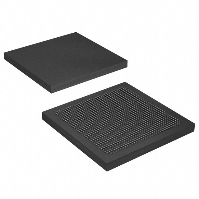
- I/O and Package — 396 I/O pins in a 1152-BBGA FCBGA package; supplied package: 1152-FBGA, FC (35×35 mm), suitable for compact, high-density board designs with surface-mount assembly.
- Transceivers and Interfaces (Family Capabilities) — Arria 10 family features include low-power serial transceivers, PCIe Gen1/Gen2/Gen3 hard IP and support for 10 Gbps Ethernet and Interlaken protocols, enabling high-speed external connectivity for networking and transport applications.
- DSP and Clocking (Family Capabilities) — Variable-precision DSP blocks and comprehensive clock networks with PLL/I/O PLL options for fractional synthesis support demanding signal-processing and timing architectures.
- Power and Voltage — Device supply operating range 870 mV–980 mV, allowing designs to target low-voltage power domains.
- Operating Range & Reliability — Industrial-grade component rated for −40 °C to 100 °C operation and RoHS compliant for regulatory alignment.
Typical Applications
- Wireless Infrastructure: Channel and switch cards in remote radio heads and mobile backhaul modules leveraging high logic density and on-chip DSP for RF baseband and control functions.
- Wireline Transport: 40G/100G muxponders, transponders and 100G line cards using built-in transceivers and PCIe hard IP for high-bandwidth packet handling and protocol conversion.
- Broadcast & Media: Studio switches, video transport and professional AV processing where embedded RAM and high I/O count support frame buffering and format conversion.
- Data Center & Storage Acceleration: Flash cache controllers and server acceleration tasks that benefit from abundant logic resources and high-speed interfaces for low-latency data paths.
- Medical & Defense Imaging: Diagnostic scanners and radar/electronic-warfare subsystems that require deterministic processing, DSP resources and wide operating temperature compliance.
Unique Advantages
- High Logic Capacity: 480,000 logic elements provide headroom for large-scale RTL designs, protocol stacks and hardware acceleration kernels.
- Substantial On-Chip Memory: Over 5.6 Mb of embedded RAM reduces dependence on external memory for buffers and short-term data retention, simplifying board-level memory architectures.
- Flexible I/O and Packaging: 396 I/O pins in a 1152-BBGA/1152-FBGA package format supports dense connector integration and compact PCB layouts.
- Industrial Temperature Range: Rated for −40 °C to 100 °C operation to support industrial and ruggedized deployments without derating core functionality.
- Low-Voltage Operation: 870 mV–980 mV supply range supports designs targeting low-power system domains and modern power management strategies.
- Arria 10 Family Capabilities: Family-level features such as variable-precision DSP blocks, advanced clocking, serial transceivers and PCIe hard IP enable integration of high-speed interfaces and compute functions on a single device.
Why Choose 10AX048K4F35I3LG?
The 10AX048K4F35I3LG combines substantial logic and memory resources with a high I/O count and industrial temperature rating, making it a strong choice for mid-range designs that require on-chip processing, protocol acceleration and high-speed connectivity. Its Arria 10 GX family heritage brings architecture-level features—DSP blocks, embedded memory types, clocking and transceiver support—that simplify integration of signal-processing and networking functions.
This device suits engineering teams and procurement focused on scalable FPGA-based solutions that balance performance and power efficiency while meeting industrial environmental and packaging requirements. Its resource set supports a wide range of applications from transport and wireless infrastructure to data-acceleration and imaging systems.
Request a quote or submit a purchasing inquiry to evaluate the 10AX048K4F35I3LG for your next design or production run.


Date Founded: 1968
Headquarters: Santa Clara, California, USA
Employees: 130,000+
Revenue: $54.23 Billion
Certifications and Memberships: ISO9001:2015, ISO14001:2015, ISO17025:2017, ISO27001:2022, ISO45001:2018, ISO50001:2018


