
10AX057K4F40I3SG
| Part Description |
Arria 10 GX Field Programmable Gate Array (FPGA) IC 696 42082304 570000 1517-BBGA, FCBGA |
|---|---|
| Quantity | 113 Available (as of June 15, 2026) |

| Product Category | Field Programmable Gate Array (FPGA) |
|---|---|
| Manufacturer | Intel |
| Manufacturing Status | Active |
| Manufacturer Standard Lead Time | 12 Weeks |
| Datasheet |
Specifications & Environmental
| Device Package | 1517-FCBGA (40x40) | Grade | Industrial | Operating Temperature | -40°C – 100°C | ||
|---|---|---|---|---|---|---|---|
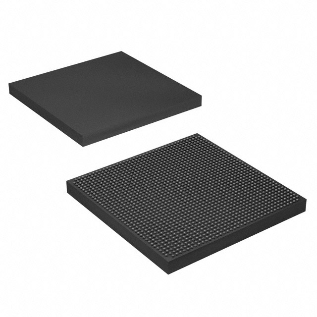
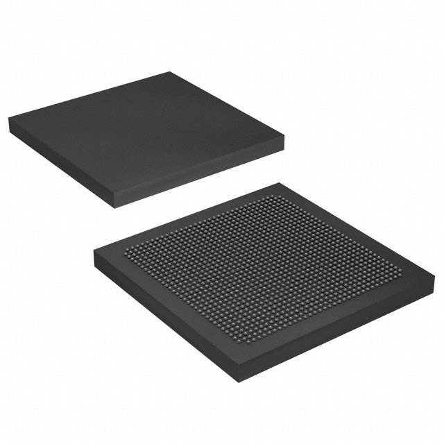
| Package / Case | 1517-BBGA, FCBGA | Number of I/O | 696 | Voltage | 870 mV - 930 mV | ||
| Mounting Method | Surface Mount | RoHS Compliance | RoHS Compliant | REACH Compliance | REACH Unaffected | ||
| Moisture Sensitivity Level | 3 (168 Hours) | Number of LABs/CLBs | 217080 | Number of Logic Elements/Cells | 570000 | ||
| Number of Gates | N/A | ECCN | 3A001A7B | HTS Code | 8542.39.0001 | ||
| Qualification | N/A | Total RAM Bits | 42082304 |
Overview of 10AX057K4F40I3SG – Arria 10 GX FPGA, 1517‑FCBGA (570000 logic elements)
The 10AX057K4F40I3SG is an Intel Arria 10 GX field‑programmable gate array (FPGA) in a 1517‑ball FCBGA (40×40) package, designed for surface‑mount placement. As part of the Arria 10 family of 20‑nm mid‑range FPGAs, it targets high‑performance, power‑sensitive designs across wireless, wireline, broadcast, computing, medical and defense markets.
With 570,000 logic elements, 42,082,304 bits of embedded RAM and 696 I/O pins, this device delivers the integration density and I/O capacity required for complex signal processing, packet processing and system‑level acceleration while operating across a wide industrial temperature and low supply‑voltage range.
Key Features
- Logic Capacity Provides 570,000 logic elements for large, complex designs and high implementation density.
- On‑Chip Memory Includes 42,082,304 bits of total embedded RAM to support buffering, packet queues and embedded data structures.
- I/O and Packaging Features 696 I/O pins in a 1517‑BBGA / 1517‑FCBGA (40×40) supplier package for broad interface connectivity; surface‑mount mounting type.
- Voltage and Power Operates from 870 mV to 930 mV supply, enabling low‑voltage system integration and power management strategies.
- Temperature and Grade Industrial grade device rated for −40 °C to 100 °C operating temperature range for deployment in demanding environments.
- RoHS Compliance RoHS‑compliant manufacturing status.
- Arria 10 Family Capabilities Arria 10 devices are described as 20‑nm mid‑range FPGAs providing higher performance and improved power efficiency; family features include variable‑precision DSP blocks, embedded memory blocks, advanced clock networks and PLLs, low‑power serial transceivers, PCIe hard IP and options for an SoC hard processor system, dynamic/partial reconfiguration and SEU detection/correction.
Typical Applications
- Wireless Infrastructure Channel and switch cards, remote radio head functions and mobile backhaul designs that require dense logic, large on‑chip memory and plentiful I/O for RF and baseband interfacing.
- Wireline and Optical Transport Line cards, muxponders and transponders (40G/100G) demanding high logic integration and embedded RAM for packet buffering and real‑time processing.
- Broadcast and Professional AV Studio switching, video transport and conferencing systems that benefit from high logic density and flexible I/O to manage multi‑channel media streams.
- Computing and Storage Acceleration Flash cache controllers, server acceleration and cloud infrastructure offload where large logic resources and on‑chip memory reduce external memory dependence.
- Medical and Defense Systems Diagnostic imaging, radar and electronic warfare subsystems that require industrial temperature operation and high integration for complex signal processing.
Unique Advantages
- High integration density: 570,000 logic elements and over 42 million bits of embedded RAM consolidate logic and memory on‑chip to reduce external BOM and board area.
- Extensive I/O footprint: 696 I/O pins in a compact 1517‑FCBGA package deliver flexible interfacing for multi‑lane SERDES, memory buses and control signals.
- Industrial‑grade operation: Specified for −40 °C to 100 °C and RoHS compliant, enabling deployment in temperature‑demanding and regulated environments.
- Low‑voltage operation: Narrow supply window (870 mV–930 mV) supports low‑power system architectures and precise power management.
- Family ecosystem and design resources: Part of the documented Arria 10 device family with established architecture features such as DSP blocks, PLLs, transceivers and hard IP for PCIe and high‑speed Ethernet, enabling reuse of design blocks and accelerators.
Why Choose 10AX057K4F40I3SG?
The 10AX057K4F40I3SG Arria 10 GX FPGA combines significant logic capacity, large embedded RAM and a broad I/O complement in a compact FCBGA package suited to industrial environments. Its family heritage emphasizes both performance and power efficiency, making it appropriate for mid‑range systems that need scalable compute and interface density without escalating board complexity.
This device is well suited to engineers designing communication infrastructure, high‑performance embedded systems and data‑processing accelerators who need a documented platform with advanced FPGA features and the capacity to implement large, memory‑intensive designs within an industrial temperature window.
Request a quote or submit an inquiry to get pricing and availability for the 10AX057K4F40I3SG Arria 10 GX FPGA.


Date Founded: 1968
Headquarters: Santa Clara, California, USA
Employees: 130,000+
Revenue: $54.23 Billion
Certifications and Memberships: ISO9001:2015, ISO14001:2015, ISO17025:2017, ISO27001:2022, ISO45001:2018, ISO50001:2018


