
10AX066H1F34E1HG
| Part Description |
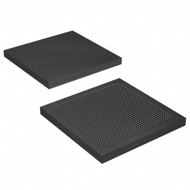
Arria 10 GX Field Programmable Gate Array (FPGA) IC 492 49610752 660000 1152-BBGA, FCBGA |
|---|---|
| Quantity | 566 Available (as of June 18, 2026) |
| Product Category | Field Programmable Gate Array (FPGA) |
|---|---|
| Manufacturer | Intel |
| Manufacturing Status | Active |
| Manufacturer Standard Lead Time | 12 Weeks |
| Datasheet |
Specifications & Environmental
| Device Package | 1152-FCBGA (35x35) | Grade | Extended | Operating Temperature | 0°C – 100°C | ||
|---|---|---|---|---|---|---|---|
| Package / Case | 1152-BBGA, FCBGA | Number of I/O | 492 | Voltage | 870 mV - 980 mV | ||
| Mounting Method | Surface Mount | RoHS Compliance | RoHS Compliant | REACH Compliance | REACH Unaffected | ||
| Moisture Sensitivity Level | 3 (168 Hours) | Number of LABs/CLBs | 250540 | Number of Logic Elements/Cells | 660000 | ||
| Number of Gates | N/A | ECCN | 5A002A1 | HTS Code | 8542.39.0001 | ||
| Qualification | N/A | Total RAM Bits | 49610752 |
Overview of 10AX066H1F34E1HG – Arria 10 GX Field Programmable Gate Array (FPGA) IC
The 10AX066H1F34E1HG is an Intel Arria 10 GX family FPGA delivering a combination of high logic capacity and embedded memory for mid-range, performance-sensitive applications. Built on the Arria 10 device architecture, this part is positioned for markets that require high-performance, power-aware programmable logic and advanced I/O.
Typical use cases include wireless and wireline communications, broadcast and video infrastructure, server acceleration and storage applications, and diagnostic imaging, where the device's density, memory, and I/O capabilities enable system-level integration and flexible interface support.
Key Features
- Process & Architecture Part of the Intel Arria 10 device family, a 20 nm mid-range FPGA architecture focused on performance and power efficiency.
- Logic Capacity 660,000 logic elements to implement complex custom logic, state machines, and datapaths.
- Embedded Memory 49,610,752 total RAM bits of on-chip memory for buffering, queues, and local storage.
- DSP & Compute Includes variable-precision DSP block capability (family feature) for flexible fixed- and floating-point signal processing.
- High-speed Serial & Protocol Support Family-level support for low-power serial transceivers, transceiver channels, PMA and PCS features, and high-speed protocols including PCIe Gen1/Gen2/Gen3 and 10 Gbps Ethernet/Interlaken hard IP.
- I/O Capacity 492 general-purpose I/O pins to support multiple external interfaces and parallel buses.
- Package & Mounting 1152-FCBGA package (35 × 35 mm) in a surface-mount form factor for compact board integration.
- Power Supported core supply range of 870 mV to 980 mV, enabling targeted power budgeting for the programmable fabric.
- Operating Range & Grade Extended-grade device with an operating temperature range of 0 °C to 100 °C.
- Compliance RoHS compliant.
Typical Applications
- Wireless infrastructure Channel and switch cards in remote radio heads and mobile backhaul designs leveraging programmable logic density and serial interfaces.
- Wireline & optical networking 40G/100G muxponders, transponders, and line cards that require high-speed transceivers and hard IP for protocol support.
- Broadcast and professional video Studio switching, transport, and videoconferencing equipment using on-chip memory and logic to handle real-time media processing.
- Computing & storage Flash caching, server acceleration, and cloud infrastructure offload where large logic capacity and embedded memory accelerate custom algorithms.
Unique Advantages
- High logic density: 660,000 logic elements enable complex system consolidation and custom hardware acceleration within a single device.
- Substantial on-chip memory: Nearly 50 million RAM bits reduce external memory dependency for buffering and intermediate storage, simplifying board design.
- Rich connectivity: 492 I/Os plus family-level high-speed transceiver and protocol hard IP support make it well-suited for multi-protocol, multi-channel systems.
- Compact package: 1152-FCBGA (35 × 35 mm) provides a high-density solder-down footprint for space-constrained PCBs.
- Power-aware platform: Arria 10 family design emphasizes power efficiency along with performance, and the part supports a core voltage range of 870 mV–980 mV for power budgeting.
- Extended operating range: 0 °C to 100 °C grade suitable for many commercial and communications applications requiring extended-temperature operation.
Why Choose 10AX066H1F34E1HG?
The 10AX066H1F34E1HG combines substantial logic capacity, extensive on-chip RAM, and a broad set of I/O and high-speed interface capabilities from the Arria 10 GX family, making it a practical choice for mid-range designs that demand programmability, integration, and protocol flexibility. Its extended temperature grade and surface-mount 1152-FCBGA package support robust board-level implementation in communications, broadcast, and compute acceleration systems.
As part of the Intel Arria 10 family, this device benefits from device-level documentation and family features such as programmable DSP resources, embedded memory configurations, and hardened protocol IP, helping teams move from prototype to deployment while keeping design complexity and BOM footprint manageable.
Request a quote or submit an inquiry for pricing and availability of 10AX066H1F34E1HG to evaluate this FPGA for your next design.


Date Founded: 1968
Headquarters: Santa Clara, California, USA
Employees: 130,000+
Revenue: $54.23 Billion
Certifications and Memberships: ISO9001:2015, ISO14001:2015, ISO17025:2017, ISO27001:2022, ISO45001:2018, ISO50001:2018


