
10AX090R1F40E1SG
| Part Description |
Arria 10 GX Field Programmable Gate Array (FPGA) IC 342 59234304 900000 1517-BBGA, FCBGA |
|---|---|
| Quantity | 125 Available (as of June 18, 2026) |

| Product Category | Field Programmable Gate Array (FPGA) |
|---|---|
| Manufacturer | Intel |
| Manufacturing Status | Active |
| Manufacturer Standard Lead Time | 9 Weeks |
| Datasheet |
Specifications & Environmental
| Device Package | 1517-FCBGA (40x40) | Grade | Extended | Operating Temperature | 0°C – 100°C | ||
|---|---|---|---|---|---|---|---|
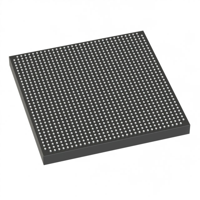
| Package / Case | 1517-BBGA, FCBGA | Number of I/O | 342 | Voltage | 870 mV - 980 mV | ||
| Mounting Method | Surface Mount | RoHS Compliance | RoHS Compliant | REACH Compliance | REACH Unaffected | ||
| Moisture Sensitivity Level | 3 (168 Hours) | Number of LABs/CLBs | 339620 | Number of Logic Elements/Cells | 900000 | ||
| Number of Gates | N/A | ECCN | 3A001A7A | HTS Code | 8542.39.0001 | ||
| Qualification | N/A | Total RAM Bits | 59234304 |
Overview of 10AX090R1F40E1SG – Arria 10 GX FPGA, 1517‑FCBGA (40×40)
The Intel Arria 10 GX 10AX090R1F40E1SG is a mid-range, 20 nm Field Programmable Gate Array (FPGA) in a 1517‑ball FCBGA package. It combines large programmable logic capacity with on‑chip memory and a broad set of series features targeted at high‑performance, power‑sensitive applications.
Designed for markets such as wireless and wireline infrastructure, broadcast, compute and storage, and specialized imaging and defense systems, this device delivers a balance of performance, integration, and power efficiency for complex system designs.
Key Features
- Logic Capacity — 900,000 logic elements for implementing large, complex designs and custom hardware acceleration.
- Logic Blocks — 339,620 logic blocks to structure and partition designs for efficient synthesis and placement.
- On‑chip Memory — 59,234,304 total RAM bits to support large buffers, caches, and memory‑centric functions without external memory for many use cases.
- I/O — 342 device I/O pins to interface with a wide variety of peripherals and high‑speed links.
- Voltage and Temperature — Core supply range 870 mV to 980 mV and an operating temperature range of 0 °C to 100 °C; suitable for extended‑grade deployments.
- Package — 1517‑BBGA / 1517‑FCBGA (40×40) surface‑mount package for high‑density board integration.
- Series‑Level IP and Resources — Arria 10 family features referenced in the device series include variable‑precision DSP blocks, multiple embedded memory block types, fractional and I/O PLLs, PCIe Gen1/Gen2/Gen3 hard IP, enhanced PCS hard IP for Interlaken and 10 Gbps Ethernet, and low‑power serial transceivers.
- Configuration and Reliability — Series documentation highlights support for dynamic and partial reconfiguration and SEU error detection and correction mechanisms.
- Environment — RoHS compliant.
- Mounting — Surface mount package suitable for modern PCB assembly processes.
Typical Applications
- Wireless Infrastructure — Channel and switch card functions in remote radio heads and mobile backhaul systems that benefit from integrated DSP and programmable logic.
- High‑Speed Networking — 40G/100G muxponder, transponder, and line‑card processing using available PCIe and high‑speed serial/PCS hard IP in the series.
- Broadcast & Pro AV — Studio switching and professional audio/video processing where on‑chip memory and DSP resources accelerate media pipelines.
- Compute & Storage Acceleration — Flash cache, server acceleration, and cloud compute functions that leverage large logic, embedded memory, and hard IP blocks.
Unique Advantages
- High Integration: Large logic element count and extensive embedded RAM reduce the need for external components and simplify board implementation.
- Balanced Performance and Power: Series positioning emphasizes improved performance with power‑saving technologies, helping designs hit performance targets while managing thermal and power budgets.
- Broad Interface Support: 342 I/O pins plus series hard IP for PCIe and high‑speed serial protocols enable flexible connectivity and high‑bandwidth data paths.
- Flexible On‑Chip Resources: DSP blocks, multiple memory block types, and PLL resources allow designers to implement a wide range of signal processing and timing architectures on a single device.
- Extended‑Grade Ready: Specified operating range of 0 °C to 100 °C and RoHS compliance suit extended‑grade electronic systems.
Why Choose 10AX090R1F40E1SG?
The 10AX090R1F40E1SG delivers a combination of large programmable logic, substantial on‑chip memory, and series‑level connectivity and IP that fit mid‑range, power‑sensitive applications requiring scalable performance. Its 1517‑ball FCBGA package and 342 I/O pins make it suitable for dense board designs where integration and I/O bandwidth matter.
This device is targeted at engineers and system designers building wireless and wireline infrastructure, broadcast processing, and data‑center acceleration solutions who need a programmable platform with substantial resources and series features such as DSP blocks, PLLs, and high‑speed serial/PCIe hard IP to accelerate development and deployment.
Request a quote or submit an inquiry to receive pricing, availability, and ordering information for the 10AX090R1F40E1SG.


Date Founded: 1968
Headquarters: Santa Clara, California, USA
Employees: 130,000+
Revenue: $54.23 Billion
Certifications and Memberships: ISO9001:2015, ISO14001:2015, ISO17025:2017, ISO27001:2022, ISO45001:2018, ISO50001:2018


