
5AGXBB1D6F31C6G
| Part Description |
Arria V GX Field Programmable Gate Array (FPGA) IC 384 17358848 300000 896-BBGA, FCBGA |
|---|---|
| Quantity | 597 Available (as of June 10, 2026) |

| Product Category | Field Programmable Gate Array (FPGA) |
|---|---|
| Manufacturer | Intel |
| Manufacturing Status | Active |
| Manufacturer Standard Lead Time | 12 Weeks |
| Datasheet |
Specifications & Environmental
| Device Package | 896-FBGA (31x31) | Grade | Commercial | Operating Temperature | 0°C – 85°C | ||
|---|---|---|---|---|---|---|---|
| Package / Case | 896-BBGA, FCBGA | Number of I/O | 384 | Voltage | 1.07 V - 1.13 V | ||
| Mounting Method | Surface Mount | RoHS Compliance | RoHS Compliant | REACH Compliance | REACH Unaffected | ||
| Moisture Sensitivity Level | 3 (168 Hours) | Number of LABs/CLBs | 14151 | Number of Logic Elements/Cells | 300000 | ||
| Number of Gates | N/A | ECCN | PENDING ECCN | HTS Code | 0000.00.0000 | ||
| Qualification | N/A | Total RAM Bits | 17358848 |
Overview of 5AGXBB1D6F31C6G – Arria V GX FPGA, 300,000 logic elements, ~17.36 Mbits RAM, 384 I/Os, 896-BBGA
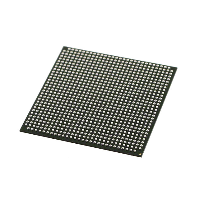
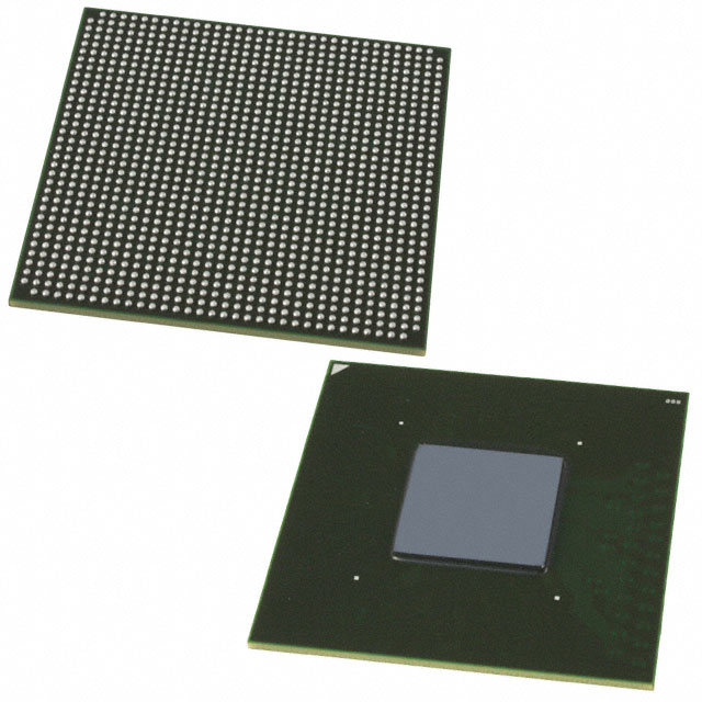
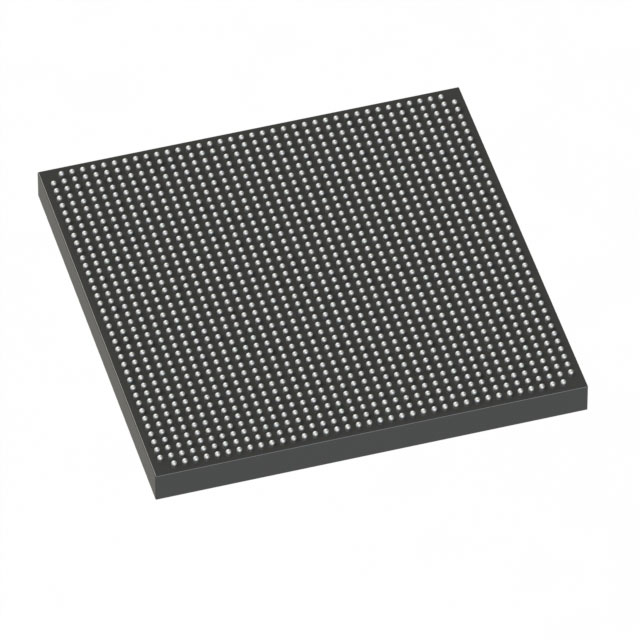
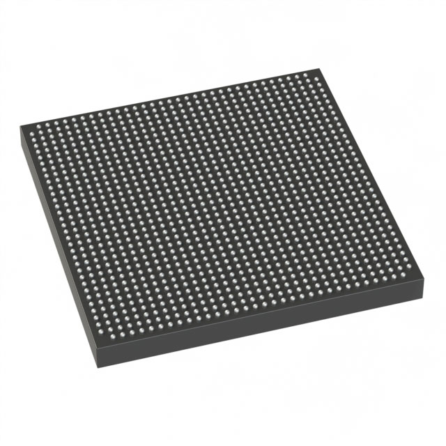
The 5AGXBB1D6F31C6G is an Intel Arria V GX field-programmable gate array (FPGA) in a 896-BBGA FCBGA package. It delivers a large programmable logic capacity and substantial on-chip memory, combined with a high I/O count and a compact surface-mount BGA footprint.
Targeted at designs that require dense logic, embedded memory, and high I/O integration, this commercial-grade device operates with a core supply between 1.07 V and 1.13 V and an operating temperature range of 0 °C to 85 °C. The device is RoHS compliant.
Key Features
- Logic Capacity Approximately 300,000 logic elements, supported by 14,151 CLB-equivalent units, for complex programmable logic implementations.
- Embedded Memory Approximately 17.36 Mbits of on-chip RAM, enabling local buffering, lookup tables, and on-chip data storage for high-throughput designs.
- I/O Density 384 user I/O pins to support wide parallel interfaces and multiple high-pin-count peripherals.
- Package & Mounting 896-BBGA (FCBGA) package, supplier device package: 896-FBGA (31×31), optimized for surface-mount PCB assembly and compact board layouts.
- Power Core voltage supply range of 1.07 V to 1.13 V for predictable power budgeting and core supply design.
- Operating Range & Grade Commercial grade device rated for 0 °C to 85 °C operation.
- Regulatory Compliance RoHS compliant, supporting regulatory and environmental requirements for many commercial applications.
Typical Applications
- High-density digital signal processing Leverage the large logic capacity and embedded memory for algorithms that require parallel computation and on-chip buffering.
- Network and packet processing High I/O count and dense logic enable implementation of packet engines, protocol parsing, and custom forwarding logic.
- Video and image processing Sufficient on-chip RAM and logic resources to implement preprocessing, frame buffering, and custom video pipelines.
- Prototyping and complex system integration Compact BGA packaging and high resource counts make this FPGA suitable for system-level prototyping and integration where board space is constrained.
Unique Advantages
- High programmable density: Large logic element count supports complex algorithms and multi-function designs without immediate need for multiple devices.
- Substantial embedded memory: Approximately 17.36 Mbits of on-chip RAM reduces reliance on external memory for many buffering and LUT needs.
- Robust I/O capability: 384 I/Os provide flexibility for parallel interfaces, multi-channel data paths, and extensive peripheral connectivity.
- Compact package: 896-BBGA (31×31) FCBGA packaging balances high-pin-count requirements with a small board footprint for space-constrained designs.
- Predictable power envelope: Narrow core voltage supply window (1.07 V–1.13 V) simplifies core power supply design and budgeting.
- Commercial-grade availability: Rated for 0 °C to 85 °C operation and RoHS compliant for broad commercial deployments.
Why Choose 5AGXBB1D6F31C6G?
The 5AGXBB1D6F31C6G Arria V GX FPGA combines a high logic element count with significant embedded memory and a large I/O complement in a compact 896-BBGA package, making it well suited for commercial designs that need high integration density and flexible I/O. Its defined core voltage range and commercial temperature rating provide predictable integration requirements for system designers.
This device is appropriate for teams building complex, scalable FPGA-based systems that demand on-chip resources and a compact board footprint, and for projects where RoHS compliance and commercial operating coverage are required.
Request a quote or submit an inquiry to receive pricing and availability information for 5AGXBB1D6F31C6G. Provide your project requirements and desired quantities to expedite a response.


Date Founded: 1968
Headquarters: Santa Clara, California, USA
Employees: 130,000+
Revenue: $54.23 Billion
Certifications and Memberships: ISO9001:2015, ISO14001:2015, ISO17025:2017, ISO27001:2022, ISO45001:2018, ISO50001:2018


