
5AGXBB7D4F35C5G
| Part Description |
Arria V GX Field Programmable Gate Array (FPGA) IC 544 2975744 504140 1152-BBGA, FCBGA |
|---|---|
| Quantity | 283 Available (as of June 15, 2026) |

| Product Category | Field Programmable Gate Array (FPGA) |
|---|---|
| Manufacturer | Intel |
| Manufacturing Status | Active |
| Manufacturer Standard Lead Time | 16 Weeks |
| Datasheet |
Specifications & Environmental
| Device Package | 1152-FBGA, FC (35x35) | Grade | Commercial | Operating Temperature | 0°C – 85°C | ||
|---|---|---|---|---|---|---|---|
| Package / Case | 1152-BBGA, FCBGA | Number of I/O | 544 | Voltage | 1.07 V - 1.13 V | ||
| Mounting Method | Surface Mount | RoHS Compliance | RoHS Compliant | REACH Compliance | REACH Unaffected | ||
| Moisture Sensitivity Level | 3 (168 Hours) | Number of LABs/CLBs | 23786 | Number of Logic Elements/Cells | 504140 | ||
| Number of Gates | N/A | ECCN | N/A | HTS Code | N/A | ||
| Qualification | N/A | Total RAM Bits | 2975744 |
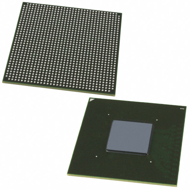
Overview of 5AGXBB7D4F35C5G – Arria V GX FPGA, 504,140 Logic Elements, 544 I/O, 1152-BBGA
The 5AGXBB7D4F35C5G is an Arria V GX field programmable gate array (FPGA) offered as a commercial-grade device in a 1152-BBGA (FCBGA) package. It provides high logic density and substantial on-chip memory with a large I/O count for designs that require extensive programmable logic and connectivity.
This device is suited to designs that demand large programmable fabric, significant embedded RAM, and a compact surface-mount BGA package while operating within a commercial temperature range and standard core-voltage window.
Key Features
- Logic Capacity — 504,140 logic elements providing high-density programmable fabric for complex logic and algorithm implementation; device listing also shows 23,786 CLBs.
- Embedded Memory — Approximately 2.98 Mbits of on-chip RAM (2,975,744 total RAM bits) to support buffer, cache, and temporary storage requirements without external memory for many functions.
- I/O Resources — 544 I/O pins to support multiple high-pin-count interfaces and system-level connectivity in a single device.
- Power Envelope — Core voltage supply specified from 1.07 V to 1.13 V, enabling precise integration with regulated power domains.
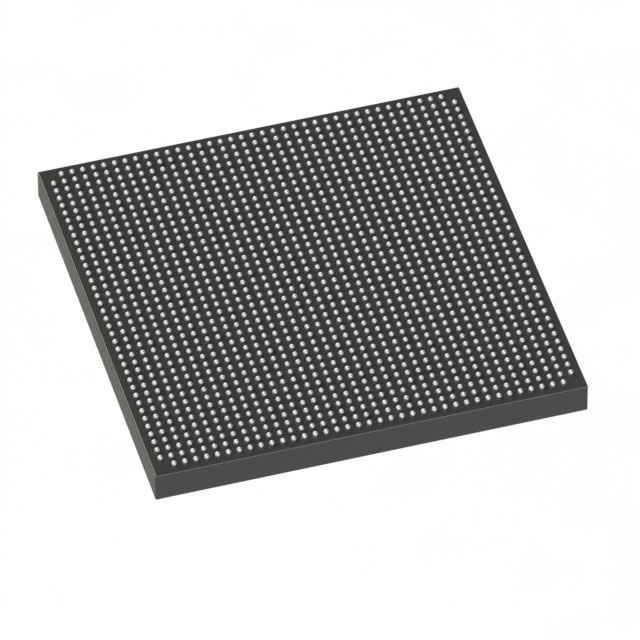
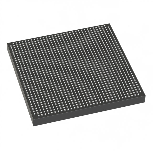
- Package & Mounting — 1152-BBGA (FCBGA) surface-mount package; supplier device package listed as 1152-FBGA, FC (35×35), suitable for dense board-level integration.
- Commercial Grade & Temperature Range — Rated for commercial operation with an operating temperature range of 0 °C to 85 °C.
- Environmental Compliance — RoHS compliant, supporting regulatory and manufacturing requirements for lead-free assembly.
Typical Applications
- High-density logic systems — Implement complex control and signal-processing algorithms using the large logic element count and abundant CLBs.
- Memory-intensive designs — Use the on-chip RAM to buffer data streams, implement FIFOs, or store intermediate datasets without immediate external memory dependence.
- High-pin-count interface bridging — Support multiple parallel or serialized interfaces and system I/Os using 544 available I/O pins in a single FPGA package.
- Compact commercial embedded systems — Integrate substantial programmable logic and I/O in a compact 1152-BBGA surface-mount package for space-constrained designs.
Unique Advantages
- High logic integration: 504,140 logic elements provide the capacity to consolidate multiple functions into a single programmable device, reducing board-level component count.
- Substantial on-chip RAM: Approximately 2.98 Mbits of embedded memory reduces reliance on external memory for many buffering and storage needs, simplifying BOM and layout.
- Extensive I/O: 544 I/O pins enable flexible connectivity for multi-interface designs and high-density peripheral integration.
- Compact BGA package: 1152-BBGA (35×35) delivers a high pin-count solution in a compact surface-mount form factor suited to modern PCB layouts.
- Commercial readiness: Rated for 0 °C to 85 °C and RoHS compliant for mainstream commercial applications and manufacturing processes.
- Controlled core-voltage range: Specified 1.07 V to 1.13 V core supply simplifies power-supply design and ensures operation within documented limits.
Why Choose 5AGXBB7D4F35C5G?
The 5AGXBB7D4F35C5G Arria V GX FPGA balances high logic density, ample embedded memory, and a large I/O complement in a single commercial-grade, surface-mount BGA package. It is positioned for designers who need to implement complex logic, handle substantial data buffering on-chip, and connect numerous interfaces without splitting functionality across multiple devices.
For engineering teams focused on scalability and consolidated designs, this device offers a predictable commercial operating range, RoHS compliance, and a compact package footprint to simplify board integration while delivering significant programmable resources.
Request a quote or submit an inquiry to receive pricing, availability, and ordering information for 5AGXBB7D4F35C5G. Provide your design requirements and quantity to get a tailored response.


Date Founded: 1968
Headquarters: Santa Clara, California, USA
Employees: 130,000+
Revenue: $54.23 Billion
Certifications and Memberships: ISO9001:2015, ISO14001:2015, ISO17025:2017, ISO27001:2022, ISO45001:2018, ISO50001:2018


