
5AGXMA5G4F31I3G
| Part Description |
Arria V GX Field Programmable Gate Array (FPGA) IC 384 13284352 190000 896-BBGA, FCBGA |
|---|---|
| Quantity | 567 Available (as of June 15, 2026) |

| Product Category | Field Programmable Gate Array (FPGA) |
|---|---|
| Manufacturer | Intel |
| Manufacturing Status | Active |
| Manufacturer Standard Lead Time | 12 Weeks |
| Datasheet |
Specifications & Environmental
| Device Package | 896-FBGA (31x31) | Grade | Industrial | Operating Temperature | -40°C – 100°C | ||
|---|---|---|---|---|---|---|---|
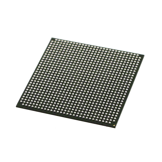
| Package / Case | 896-BBGA, FCBGA | Number of I/O | 384 | Voltage | 1.12 V - 1.18 V | ||
| Mounting Method | Surface Mount | RoHS Compliance | RoHS Compliant | REACH Compliance | REACH Unaffected | ||
| Moisture Sensitivity Level | 3 (168 Hours) | Number of LABs/CLBs | 8962 | Number of Logic Elements/Cells | 190000 | ||
| Number of Gates | N/A | ECCN | PENDING ECCN | HTS Code | 0000.00.0000 | ||
| Qualification | N/A | Total RAM Bits | 13284352 |
Overview of 5AGXMA5G4F31I3G – Arria V GX Field Programmable Gate Array (FPGA) IC
The 5AGXMA5G4F31I3G is an Arria V GX Field Programmable Gate Array (FPGA) in an 896‑BBGA FCBGA package, offering high logic density and abundant I/O in a surface‑mount form factor. Designed for industrial‑grade applications, this device provides a combination of on‑chip memory, logic resources, and a wide operating temperature range.
With 190,000 logic elements, approximately 13.3 Mbits of embedded memory and 384 I/O pins, the device targets designs that require significant programmable logic capacity and extensive peripheral connectivity while operating from a core supply between 1.12 V and 1.18 V.
Key Features
- High Logic Capacity — 190,000 logic elements to implement complex digital functions and system-on-chip architectures.
- Embedded Memory — Approximately 13.3 Mbits of on‑chip RAM for buffering, lookup tables and state storage.
- Extensive I/O — 384 I/O pins to support wide peripheral and interface connectivity requirements.
- Industrial Temperature Range — Rated for operation from −40 °C to 100 °C, suitable for industrial deployments.
- Power and Voltage — Core supply specified at 1.12 V to 1.18 V to match system power architectures.
- Package and Mounting — 896‑BBGA (FCBGA) package, supplier package 896‑FBGA (31×31), designed for surface‑mount PCB assembly.
- Regulatory Compliance — RoHS compliant.
- Comprehensive Documentation — Supported by the Arria V device datasheet covering electrical characteristics, configuration timing and I/O specifications.
Typical Applications
- Industrial Systems — Deploy in industrial control and automation equipment that require industrial temperature operation and robust I/O connectivity.
- High‑Density Logic Designs — Implement complex programmable logic functions using the device’s 190,000 logic elements.
- Memory‑Centric Algorithms — Use the device’s approximately 13.3 Mbits of embedded RAM for buffering, tables and stateful processing.
- System Integration and Prototyping — Leverage the 384 I/O and compact FCBGA package for board‑level integration and prototype development.
Unique Advantages
- High integration density: 190,000 logic elements reduce the need for multiple discrete devices and simplify system architecture.
- On‑chip memory at scale: Approximately 13.3 Mbits of embedded RAM enables local storage for latency‑sensitive tasks and data buffering.
- Broad I/O count: 384 I/O pins provide flexible connectivity for peripherals, sensors and custom interfaces.
- Industrial reliability: Rated for −40 °C to 100 °C operation, supporting deployments in demanding thermal environments.
- Compact surface‑mount package: 896‑BBGA (31×31) package balances footprint and routing density for modern PCBs.
- Standards‑aware sourcing: RoHS compliance assists with regulatory and manufacturing policies.
Why Choose 5AGXMA5G4F31I3G?
The 5AGXMA5G4F31I3G Arria V GX FPGA combines substantial logic resources, sizeable embedded memory and a high I/O count in a single industrial‑rated surface‑mount package. It is positioned for designs that demand on‑chip programmability and scalable digital resources while maintaining industrial temperature tolerance and a compact board footprint.
This device is suitable for engineering teams building mid‑to‑high complexity systems that require integrated logic and memory, deterministic I/O capacity, and the reliability expected from industrial‑grade components. Detailed electrical and configuration specifications are available in the Arria V device datasheet to support design, validation and production planning.
Request a quote or submit a procurement inquiry to obtain pricing, lead times and availability for the 5AGXMA5G4F31I3G Arria V GX FPGA.


Date Founded: 1968
Headquarters: Santa Clara, California, USA
Employees: 130,000+
Revenue: $54.23 Billion
Certifications and Memberships: ISO9001:2015, ISO14001:2015, ISO17025:2017, ISO27001:2022, ISO45001:2018, ISO50001:2018


