
5AGXMA5G4F31I3N
| Part Description |
Arria V GX Field Programmable Gate Array (FPGA) IC 384 13284352 190000 896-BBGA, FCBGA |
|---|---|
| Quantity | 338 Available (as of June 18, 2026) |

| Product Category | Field Programmable Gate Array (FPGA) |
|---|---|
| Manufacturer | Intel |
| Manufacturing Status | Obsolete |
| Manufacturer Standard Lead Time | Contact Us |
| Datasheet |
Specifications & Environmental
| Device Package | 896-FBGA (31x31) | Grade | Industrial | Operating Temperature | -40°C – 100°C | ||
|---|---|---|---|---|---|---|---|
| Package / Case | 896-BBGA, FCBGA | Number of I/O | 384 | Voltage | 1.12 V - 1.18 V | ||
| Mounting Method | Surface Mount | RoHS Compliance | RoHS Compliant | REACH Compliance | REACH Unknown | ||
| Moisture Sensitivity Level | 3 (168 Hours) | Number of LABs/CLBs | 8962 | Number of Logic Elements/Cells | 190000 | ||
| Number of Gates | N/A | ECCN | 3A001A2C | HTS Code | 8542.39.0001 | ||
| Qualification | N/A | Total RAM Bits | 13284352 |
Overview of 5AGXMA5G4F31I3N – Arria V GX FPGA, 190,000 logic elements, 896‑BBGA
The 5AGXMA5G4F31I3N is an Intel Arria V GX Field Programmable Gate Array (FPGA) offered in an industrial grade package. It delivers high programmable logic capacity, substantial on‑chip memory, and a large complement of I/O, enabling complex, I/O‑rich designs.
Designed for applications that require a combination of logic density, embedded RAM, and robust operating conditions, this device provides a platform for custom hardware acceleration, protocol consolidation, and industrial control implementations.
Key Features
- Core Logic Approximately 190,000 logic elements (logic cells) to implement high‑density custom logic and datapath designs.
- Embedded Memory Approximately 13.3 Mbits of on‑chip RAM (13,284,352 total RAM bits) for buffering, FIFOs, and local data storage.
- I/O Resources 384 user I/O pins to support wide peripheral and interface connectivity directly from the FPGA.
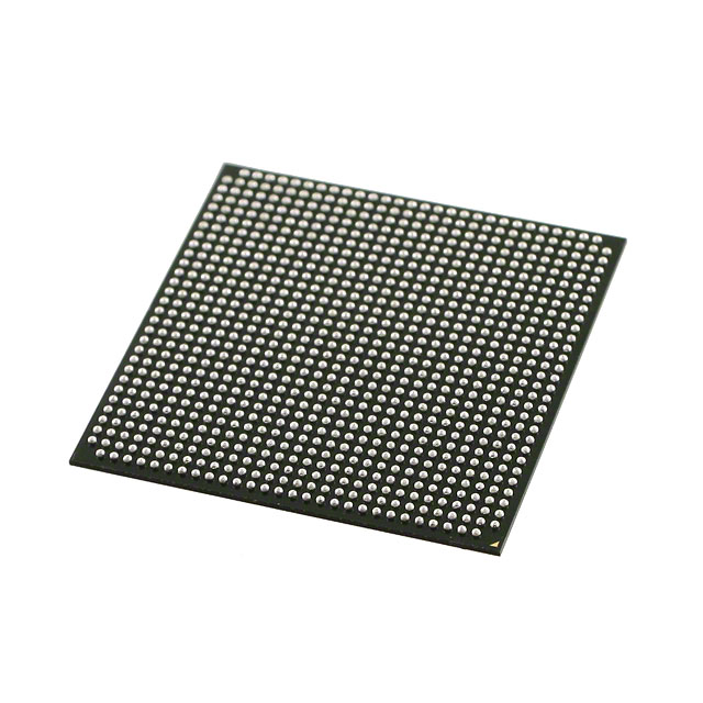
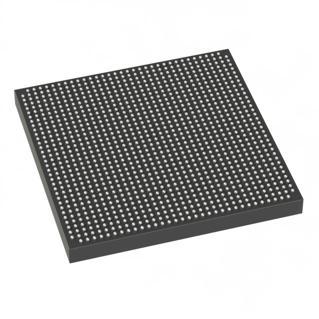
- Package & Mounting 896‑BBGA (FCBGA) package; supplier device package listed as 896‑FBGA (31×31). Surface mount for compact board integration.
- Power Core voltage supply range: 1.12 V to 1.18 V to match system power rails and power‑management design.
- Industrial Temperature Range Rated for operation from −40 °C to 100 °C, suitable for demanding environmental conditions.
- Compliance RoHS‑compliant manufacturing status.
Typical Applications
- Custom compute acceleration Use the device’s large logic array and embedded RAM to offload compute‑intensive kernels or bespoke hardware functions.
- I/O consolidation and protocol bridging Leverage 384 I/O to integrate multiple interfaces and translate between protocols on a single FPGA.
- Industrial control and automation Industrial temperature rating and substantial logic capacity support control, signal processing, and real‑time decision logic in factory and process environments.
- Test and measurement systems Implement complex timing, data capture, and preprocessing functions using on‑chip memory and dense logic resources.
Unique Advantages
- High logic capacity: Large programmable logic resource (≈190k logic elements) enables complex, parallel architectures without partitioning across multiple devices.
- Significant embedded memory: Approximately 13.3 Mbits of on‑chip RAM reduces dependency on external memory for many buffering and staging tasks.
- Abundant I/O: 384 I/O pins simplify board‑level integration by accommodating multiple peripherals and high‑pin‑count interfaces directly.
- Industrial robustness: −40 °C to 100 °C operating range and industrial grade classification support deployment in harsh environments.
- Compact FCBGA footprint: 896‑ball FCBGA (31×31) provides a high‑density package option for space‑constrained PCBs while retaining extensive I/O and logic resources.
Why Choose 5AGXMA5G4F31I3N?
The 5AGXMA5G4F31I3N Arria V GX FPGA combines substantial logic density, multi‑megabit embedded RAM, and hundreds of I/O in an industrial‑rated, surface‑mount FCBGA package. Its electrical and thermal specifications (1.12–1.18 V core supply, −40 °C to 100 °C operation) make it well suited for system designs that demand high integration and reliable operation across challenging environments.
Backed by Arria V family documentation, the device is appropriate for engineers and procurement teams building scalable, high‑function FPGA solutions where on‑chip resources and industrial operating range are key selection criteria.
Request a quote or submit an inquiry to receive pricing and availability information for the 5AGXMA5G4F31I3N Arria V GX FPGA.


Date Founded: 1968
Headquarters: Santa Clara, California, USA
Employees: 130,000+
Revenue: $54.23 Billion
Certifications and Memberships: ISO9001:2015, ISO14001:2015, ISO17025:2017, ISO27001:2022, ISO45001:2018, ISO50001:2018


