
5AGXMB7G4F40C5G
| Part Description |
Arria V GX Field Programmable Gate Array (FPGA) IC 704 2975744 504140 1517-BBGA, FCBGA |
|---|---|
| Quantity | 1,499 Available (as of June 15, 2026) |

| Product Category | Field Programmable Gate Array (FPGA) |
|---|---|
| Manufacturer | Intel |
| Manufacturing Status | Active |
| Manufacturer Standard Lead Time | 16 Weeks |
| Datasheet |
Specifications & Environmental
| Device Package | 1517-FBGA, FC (40x40) | Grade | Commercial | Operating Temperature | 0°C – 85°C | ||
|---|---|---|---|---|---|---|---|
| Package / Case | 1517-BBGA, FCBGA | Number of I/O | 704 | Voltage | 1.07 V - 1.13 V | ||
| Mounting Method | Surface Mount | RoHS Compliance | RoHS Compliant | REACH Compliance | REACH Unaffected | ||
| Moisture Sensitivity Level | 3 (168 Hours) | Number of LABs/CLBs | 23786 | Number of Logic Elements/Cells | 504140 | ||
| Number of Gates | N/A | ECCN | N/A | HTS Code | N/A | ||
| Qualification | N/A | Total RAM Bits | 2975744 |
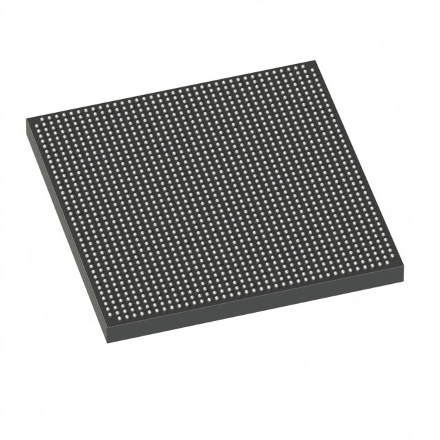
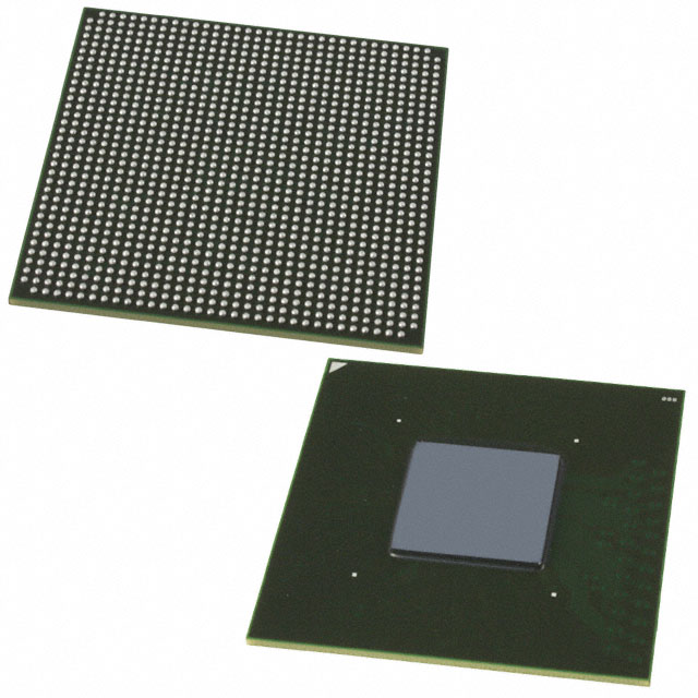
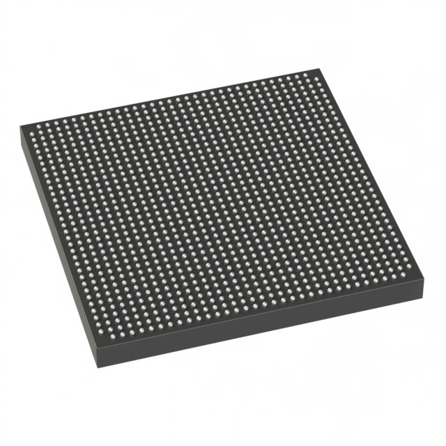
Overview of 5AGXMB7G4F40C5G – Arria V GX FPGA (504,140 logic elements, 704 I/O, 1517-BBGA FCBGA)
The 5AGXMB7G4F40C5G is an Intel Arria V GX field-programmable gate array (FPGA) in a 1517‑BBGA FCBGA package. It delivers high-density programmable logic with 504,140 logic elements and approximately 2.98 Mbits of embedded memory, together with 704 general-purpose I/O pins.
This commercial‑grade device (0 °C to 85 °C) targets designs that require large on‑chip logic capacity, substantial embedded RAM, and extensive I/O resources while operating from a core supply in the 1.07 V to 1.13 V range. Detailed electrical, configuration, and timing specifications are provided in the Arria V device datasheet.
Key Features
- High-density logic 504,140 logic elements to support complex digital designs and large custom logic implementations.
- Embedded memory Approximately 2.98 Mbits of on‑chip RAM for buffering, packet storage, or scratch memory without external RAM dependency.
- Extensive I/O 704 I/O pins for broad peripheral connectivity and multi‑lane interfaces.
- Package and mounting 1517‑BBGA (FCBGA) package; supplier device package listed as 1517‑FBGA, FC (40×40); surface mount for board‑level integration.
- Power and operating conditions Core voltage supply specified between 1.07 V and 1.13 V; commercial operating temperature range 0 °C to 85 °C.
- Standards compliance RoHS compliant, supporting lead‑free manufacturing requirements.
- Comprehensive documentation Supported by the Arria V device datasheet covering electrical characteristics, switching characteristics, configuration specifications, and I/O timing.
Typical Applications
- Custom digital hardware Implement large, application‑specific logic blocks and control functions using the device’s high logic element count and on‑chip memory.
- High‑pin‑count interface aggregation Consolidate multiple peripheral and protocol interfaces leveraging up to 704 I/Os.
- Prototyping and system validation Use the device for complex prototype systems requiring substantial programmable resources and flexible I/O assignments.
Unique Advantages
- High logic capacity: 504,140 logic elements enable large-scale custom logic integration without immediate dependence on external logic devices.
- On‑chip memory for system tasks: Approximately 2.98 Mbits of embedded RAM reduces external memory bandwidth requirements for buffering and intermediate storage.
- Broad I/O availability: 704 I/Os allow flexible partitioning of signals and support for multi‑channel or multi‑protocol designs.
- Commercial temperature rating: Specified 0 °C to 85 °C operation for standard commercial applications and environments.
- Surface‑mount, compact package: 1517‑BBGA FCBGA footprint provides a high‑pin‑count solution in a board‑mountable package.
- Regulatory compatibility: RoHS compliance simplifies integration into lead‑free manufacturing flows.
Why Choose 5AGXMB7G4F40C5G?
The 5AGXMB7G4F40C5G Arria V GX FPGA combines very large logic capacity, significant embedded memory, and extensive I/O in a surface‑mount 1517‑BBGA package. Its electrical operating range and the comprehensive Arria V device datasheet make it suitable for demanding commercial designs that require on‑chip resources and flexible interfacing.
This device is well suited for development teams and system designers looking to consolidate complex logic, memory buffering, and multi‑signal connectivity into a single programmable device while relying on documented device electrical and configuration specifications.
Request a quote or submit a request to obtain pricing, availability, and lead‑time information for the 5AGXMB7G4F40C5G Arria V GX FPGA.


Date Founded: 1968
Headquarters: Santa Clara, California, USA
Employees: 130,000+
Revenue: $54.23 Billion
Certifications and Memberships: ISO9001:2015, ISO14001:2015, ISO17025:2017, ISO27001:2022, ISO45001:2018, ISO50001:2018


