
5SEEBF45I2N
| Part Description |
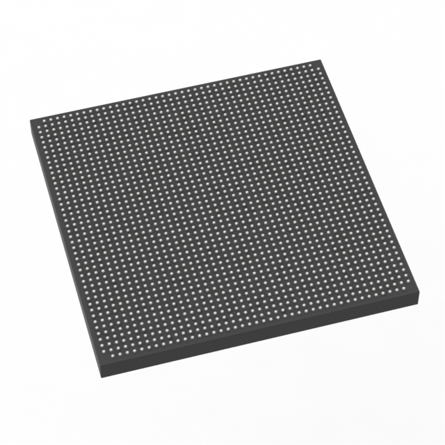
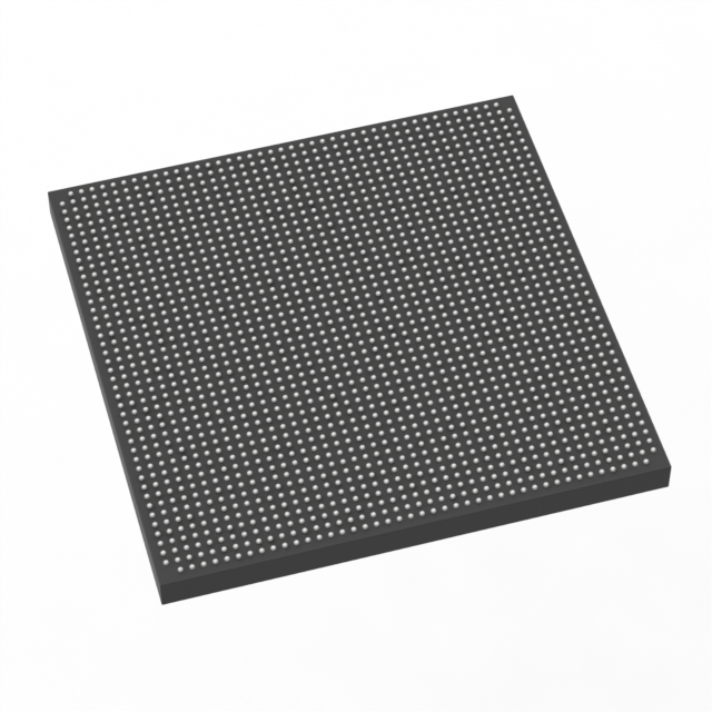
Stratix® V E Field Programmable Gate Array (FPGA) IC 840 53248000 952000 1932-BBGA, FCBGA |
|---|---|
| Quantity | 1,254 Available (as of October 8, 2026) |
| Product Category | Field Programmable Gate Array (FPGA) |
|---|---|
| Manufacturer | Intel |
| Manufacturing Status | Obsolete |
| Manufacturer Standard Lead Time | Contact Us |
| Datasheet |
Specifications & Environmental
| Device Package | 1932-FBGA, FC (45x45) | Grade | Industrial | Operating Temperature | -40°C – 100°C | ||
|---|---|---|---|---|---|---|---|
| Package / Case | 1932-BBGA, FCBGA | Number of I/O | 840 | Voltage | 870 mV - 930 mV | ||
| Mounting Method | Surface Mount | RoHS Compliance | RoHS Compliant | REACH Compliance | REACH Unknown | ||
| Moisture Sensitivity Level | 3 (168 Hours) | Number of LABs/CLBs | 359250 | Number of Logic Elements/Cells | 952000 | ||
| Number of Gates | N/A | ECCN | 3A001A2C | HTS Code | 8542.39.0001 | ||
| Qualification | N/A | Total RAM Bits | 53248000 |
Overview of 5SEEBF45I2N – Stratix® V E FPGA, 952k Logic Elements
The 5SEEBF45I2N is an Intel Stratix V E field-programmable gate array (FPGA) optimized for designs that require very high logic density and extensive on-chip memory. Built on a 28‑nm TSMC process, this Stratix V E device targets applications such as ASIC and system emulation, diagnostic imaging, and instrumentation where large logic capacity and deterministic I/O are needed.
This device combines nearly one million logic elements, a large pool of embedded RAM, and a high I/O count in a 1932‑ball FCBGA package, delivering a scalable platform for complex, data‑intensive FPGA designs.
Key Features
- Core Architecture 28‑nm TSMC process technology with a documented core supply range of 870 mV to 930 mV; Stratix V family enhancements include an adaptive logic module (ALM) and a comprehensive fabric clocking network.
- Logic Capacity 952,000 logic elements, providing the logic density required for large, complex designs.
- On‑chip Memory Approximately 53.2 Mbits of embedded memory (total RAM bits: 53,248,000), supported by 20‑Kbit M20K memory blocks in the Stratix V architecture.
- DSP and Timing Resources Variable‑precision DSP blocks and fractional PLLs provide high‑performance signal processing and flexible clocking options.
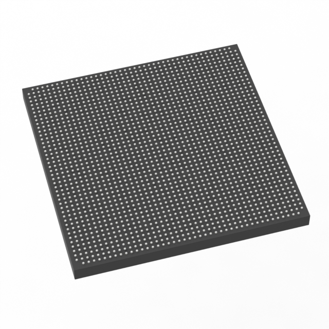
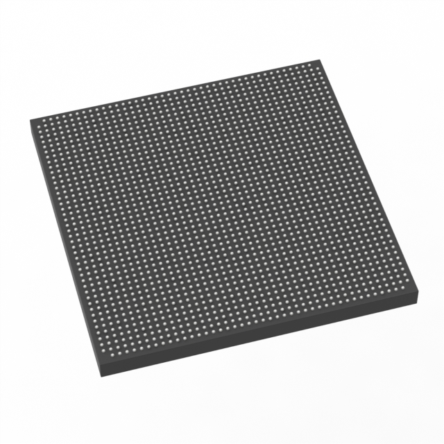
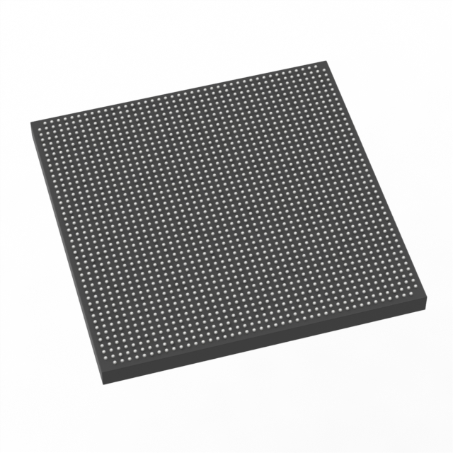
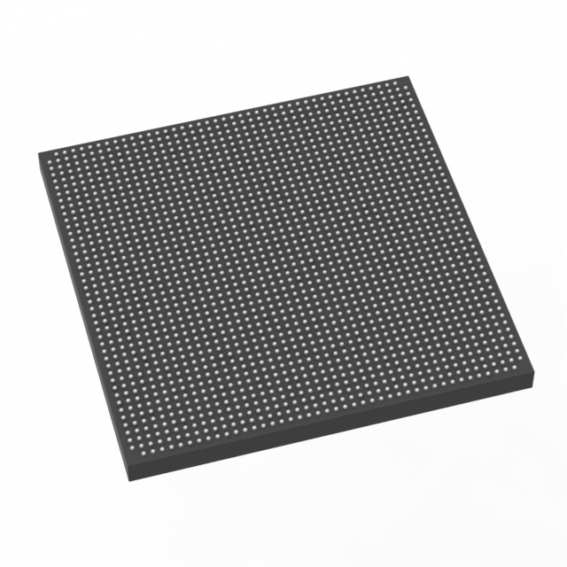
- I/O and Packaging 840 user I/Os in a 1932‑BBGA FCBGA package (supplier package: 1932‑FBGA, FC, 45×45 mm), optimized for dense board integration and surface‑mount assembly.
- Industrial Temperature Grade Rated for operation from −40 °C to 100 °C, suitable for industrial environments.
- Hard IP and Production Path Includes Embedded HardCopy Block capability for hardened IP instantiation (example: PCIe Gen3/Gen2/Gen1 hardening) and supports a low‑risk, low‑cost migration path to HardCopy V ASICs for higher volume production.
- Standards and Compliance RoHS compliant.
Typical Applications
- ASIC and System Emulation High logic density and large embedded memory make this device well suited for prototyping and emulation of ASICs and complex SoCs.
- Diagnostic Imaging Large logic resources and ample on‑chip RAM support the processing pipelines required in medical and industrial imaging systems.
- Instrumentation and Test Equipment Deterministic I/O and dense logic enable implementation of high‑channel count measurement, control, and analysis functions.
- Data‑Intensive DSP Variable‑precision DSP blocks and substantial memory support demanding digital signal processing tasks.
Unique Advantages
- Very High Logic Density: 952,000 logic elements provide the footprint to consolidate complex functions onto a single FPGA, reducing board-level partitioning.
- Large Embedded Memory: Approximately 53.2 Mbits of on‑chip RAM minimizes external memory dependency and simplifies system memory architecture.
- Extensive I/O in a Compact Package: 840 I/Os in a 1932‑ball FCBGA (45×45 mm) package offers high pin count without an oversized board footprint.
- Industrial Temperature Range: Rated −40 °C to 100 °C for reliable operation in industrial environments.
- Production Scalability: Embedded HardCopy Block and documented migration path to HardCopy V ASICs support cost and risk reduction for volume production.
- Standards‑Aware Architecture: Stratix V architecture includes hard IP support (for example, PCIe generations) and mature fabric building blocks to accelerate development.
Why Choose 5SEEBF45I2N?
The 5SEEBF45I2N positions itself as a high‑density, production‑ready Stratix V E FPGA for designs that demand extensive logic, sizable embedded memory, and a large number of I/Os in a compact, surface‑mount package. Its industrial temperature rating and RoHS compliance make it suitable for demanding environments where reliability matters.
Engineers targeting ASIC prototyping, system emulation, high‑precision DSP, or instrumentation will find the device’s combination of logic capacity, on‑chip RAM, and embedded hard IP useful for reducing board complexity and accelerating time to market, with a documented path to HardCopy V ASICs for volume production.
Request a quote or submit a purchase inquiry to receive pricing, availability, and lead‑time information for the 5SEEBF45I2N.





















Date Founded: 1968
Headquarters: Santa Clara, California, USA
Employees: 130,000+
Revenue: $54.23 Billion
Certifications and Memberships: ISO9001:2015, ISO14001:2015, ISO17025:2017, ISO27001:2022, ISO45001:2018, ISO50001:2018


