
5SGSED8K2F40C2LN
| Part Description |
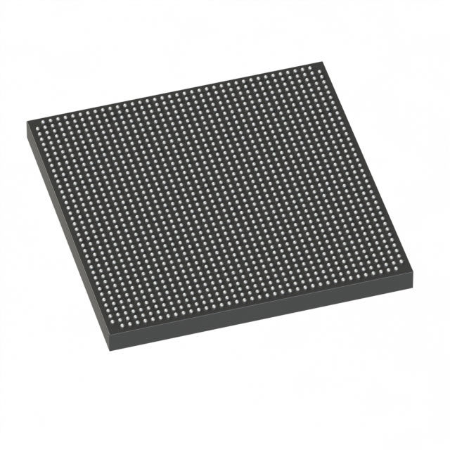
Stratix® V GS Field Programmable Gate Array (FPGA) IC 696 51200000 695000 1517-BBGA, FCBGA |
|---|---|
| Quantity | 585 Available (as of June 16, 2026) |

| Product Category | Field Programmable Gate Array (FPGA) |
|---|---|
| Manufacturer | Intel |
| Manufacturing Status | Obsolete |
| Manufacturer Standard Lead Time | Contact Us |
| Datasheet |
Specifications & Environmental
| Device Package | 1517-FBGA (40x40) | Grade | Commercial | Operating Temperature | 0°C – 85°C | ||
|---|---|---|---|---|---|---|---|
| Package / Case | 1517-BBGA, FCBGA | Number of I/O | 696 | Voltage | 820 mV - 880 mV | ||
| Mounting Method | Surface Mount | RoHS Compliance | RoHS Compliant | REACH Compliance | REACH Unknown | ||
| Moisture Sensitivity Level | 3 (168 Hours) | Number of LABs/CLBs | 262400 | Number of Logic Elements/Cells | 695000 | ||
| Number of Gates | N/A | ECCN | 3A001A2C | HTS Code | 8542.39.0001 | ||
| Qualification | N/A | Total RAM Bits | 51200000 |
Overview of 5SGSED8K2F40C2LN – Stratix V GS FPGA, 695,000 logic elements
The 5SGSED8K2F40C2LN is a Stratix® V GS field programmable gate array (FPGA) in a 1517-BBGA (FCBGA) package, offering 695,000 logic elements and approximately 51.2 Mbits of embedded memory. Built on the Stratix V family architecture, this commercial-grade device targets data‑intensive and DSP‑centric designs where high logic density, abundant on-chip memory, and dense I/O counts are required.
With up to 696 I/Os, variable‑precision DSP capability, and GS‑class transceiver support, this device is positioned for applications that require integrated DSP resources, high channel counts, and a migration path to hard‑IP ASIC implementations.
Key Features
- Core Logic 695,000 logic elements provide high logic density for complex FPGA designs.
- Embedded Memory Approximately 51.2 Mbits of on-chip RAM (Total RAM bits: 51,200,000) organized in M20K-style memory blocks as part of the Stratix V architecture.
- DSP Resources Stratix V GS devices include variable-precision DSP blocks; GS devices support up to 3,926 18×18 or 1,963 27×27 multipliers for high‑precision signal processing workloads.
- Transceivers & I/O Up to 696 I/Os and integrated transceivers (GS variant) with 14.1 Gbps data‑rate capability, enabling high-bandwidth backplane and optical interface applications.
- Power & Voltage Core supply range specified at 820 mV to 880 mV, enabling optimized core power design and supply selection.
- Package & Mounting 1517‑BBGA (FCBGA) package, supplier device package 1517‑FBGA (40×40), surface‑mount device suitable for standard PCB assembly.
- Operating Range Commercial grade operation from 0 °C to 85 °C, designed for typical commercial electronics environments.
- Standards & Compliance RoHS compliant.
Typical Applications
- High‑performance DSP systems Leverage the variable‑precision DSP blocks and dense multiplier counts for signal processing, filtering, and real‑time compute tasks.
- Optical and backplane communications Use GS‑class transceivers and high I/O density for 40G/100G backplane or optical interface implementations.
- Network processing and packet handling Deploy the large logic capacity and abundant I/O for packet classification, traffic management, and layer‑processing functions.
- Prototype-to-ASIC development Prototype production designs on Stratix V FPGAs with a documented low‑risk migration path to HardCopy V ASICs for volume production.
Unique Advantages
- High logic capacity: 695,000 logic elements support large, complex designs without immediately resorting to multi‑device solutions.
- Substantial embedded memory: Approximately 51.2 Mbits of on‑chip RAM reduces external memory dependency for buffering and on‑chip data storage.
- DSP‑oriented architecture: GS variant DSP multipliers and variable‑precision blocks provide efficient hardware for compute‑intensive signal processing.
- Dense I/O and transceiver capability: 696 I/Os and integrated 14.1 Gbps transceivers enable high channel counts and high‑speed serial interfaces in a single device.
- Commercial availability and compliance: Surface‑mount 1517‑BBGA package and RoHS compliance simplify procurement and assembly for commercial products.
- Proven family and migration path: Part of the Stratix V family with an established path to HardCopy V ASICs for cost and volume optimization.
Why Choose 5SGSED8K2F40C2LN?
The 5SGSED8K2F40C2LN combines high logic density, sizable on‑chip memory, extensive DSP resources, and dense I/O in a commercial‑grade Stratix V GS FPGA package. It is suited for designers building data‑intensive, DSP‑centric, or transceiver‑heavy systems who require a single‑device solution with a clear production migration path.
This device is appropriate for engineering teams focused on scalable performance, integration of high‑speed interfaces, and designs that may benefit from prototyping on FPGA before transitioning to HardCopy ASIC implementations.
If you require pricing, availability, or a formal quote for the 5SGSED8K2F40C2LN, submit a request and our team will provide a quote and additional purchasing information.


Date Founded: 1968
Headquarters: Santa Clara, California, USA
Employees: 130,000+
Revenue: $54.23 Billion
Certifications and Memberships: ISO9001:2015, ISO14001:2015, ISO17025:2017, ISO27001:2022, ISO45001:2018, ISO50001:2018


