
5SGSED8K2F40I3
| Part Description |
Stratix® V GS Field Programmable Gate Array (FPGA) IC 696 51200000 695000 1517-BBGA, FCBGA |
|---|---|
| Quantity | 542 Available (as of June 15, 2026) |

| Product Category | Field Programmable Gate Array (FPGA) |
|---|---|
| Manufacturer | Intel |
| Manufacturing Status | Obsolete |
| Manufacturer Standard Lead Time | Contact Us |
| Datasheet |
Specifications & Environmental
| Device Package | 1517-FBGA (40x40) | Grade | Industrial | Operating Temperature | -40°C – 100°C | ||
|---|---|---|---|---|---|---|---|
| Package / Case | 1517-BBGA, FCBGA | Number of I/O | 696 | Voltage | 820 mV - 880 mV | ||
| Mounting Method | Surface Mount | RoHS Compliance | RoHS non-compliant | REACH Compliance | REACH Unknown | ||
| Moisture Sensitivity Level | 3 (168 Hours) | Number of LABs/CLBs | 262400 | Number of Logic Elements/Cells | 695000 | ||
| Number of Gates | N/A | ECCN | 3A001A7A | HTS Code | 8542.39.0001 | ||
| Qualification | N/A | Total RAM Bits | 51200000 |
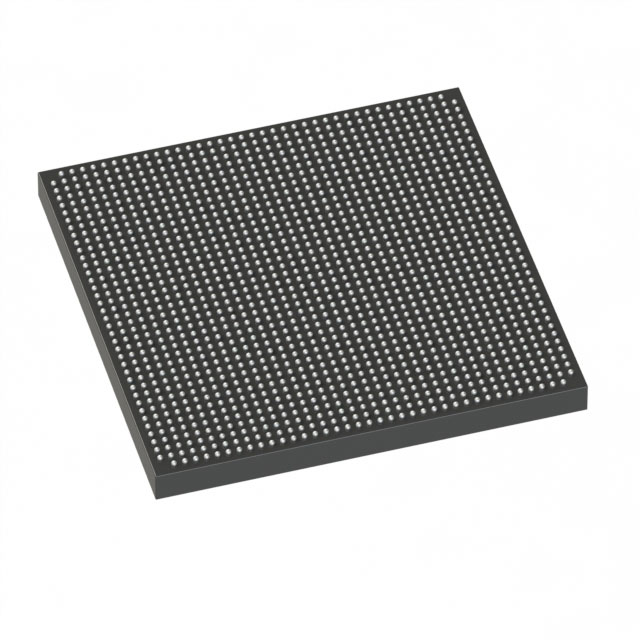
Overview of 5SGSED8K2F40I3 – Stratix® V GS FPGA, 695,000 logic elements, 1517-BBGA
The 5SGSED8K2F40I3 is a Stratix® V GS Field Programmable Gate Array (FPGA) offering a high-density, DSP-optimized architecture for transceiver‑based, signal‑processing applications. Built on a 28‑nm process with integrated hard IP and transceiver capability, this device targets bandwidth- and DSP‑centric markets such as wireline, military, broadcast, and high‑performance computing.
With approximately 695,000 logic elements, roughly 51.2 Mbits of embedded memory, abundant DSP resources, and 696 I/Os in a 1517‑FBGA package, this industrial‑grade FPGA is specified for -40°C to 100°C operation and a core supply range of 820 mV to 880 mV.
Key Features
- Core & Process 28‑nm device architecture with enhanced core building blocks and support for embedded hard IP blocks, providing a foundation for high‑performance system designs.
- Logic Density Approximately 695,000 logic elements to implement complex control, routing, and custom logic functions.
- Memory Approximately 51.2 Mbits of embedded memory supported by the family’s 20‑Kbit (M20K) memory architecture for data buffering and packet handling.
- DSP Resources GS‑family devices include variable‑precision DSP blocks supporting up to 3,926 18×18 or 1,963 27×27 multipliers, enabling high‑precision, high‑throughput signal processing.
- I/O & Transceivers 696 total I/Os in a high‑pin FCBGA package; GS devices provide integrated transceivers with 14.1‑Gbps data‑rate capability for backplane and optical interfaces.
- Power Core supply voltage specified from 820 mV to 880 mV, enabling predictable power budgeting for system designs.
- Package & Mounting 1517‑BBGA (1517‑FBGA, 40×40) FCBGA package, surface‑mount mounting for compact, high‑density board implementations.
- Temperature & Grade Industrial grade with operating temperature range from -40°C to 100°C for demanding environments.
- Environmental Compliance RoHS compliant.
Typical Applications
- High‑performance DSP systems — Deploy variable‑precision DSP blocks and abundant multipliers for signal conditioning, filtering, and high‑precision computation.
- Optical and backplane communications — Use integrated 14.1‑Gbps transceivers and large on‑chip memory for 40G/100G class transport and packet processing.
- Military and broadcast systems — Industrial operating range and high logic/DSP density support real‑time processing and ruggedized applications.
- PCIe‑based bandwidth‑centric designs — Leverage embedded hard IP and connectivity options for PCIe Gen implementations and high‑throughput I/O.
Unique Advantages
- High logic capacity: Approximately 695,000 logic elements enable integration of large custom FPGA fabrics without external logic.
- Extensive DSP resources: Thousands of dedicated multipliers provide scalable performance for compute‑intensive signal processing tasks.
- Integrated high‑speed I/O: 696 I/Os and GS‑class transceivers at 14.1 Gbps support demanding interface and bandwidth requirements.
- Substantial on‑chip memory: Approximately 51.2 Mbits of embedded RAM reduces external memory dependence for buffering and packet handling.
- Industrial‑rated operation: Specified for -40°C to 100°C to meet environmental requirements for deployed systems.
- Production scalability: Stratix V FPGAs provide a documented path to HardCopy V ASICs for low‑risk migration to higher‑volume production.
Why Choose 5SGSED8K2F40I3?
The 5SGSED8K2F40I3 combines high logic density, abundant DSP multipliers, significant embedded memory, and extensive I/O/transceiver capability in a single industrial‑grade FPG A. It is well suited for designers building transceiver‑based, DSP‑intensive systems that require a compact, high‑performance programmable fabric.
This Stratix® V GS device is positioned for engineers and procurement teams seeking a robust, scalable FPGA platform with clear production migration options and predictable electrical and environmental specifications.
Request a quote or submit a pricing and availability inquiry to start integrating the 5SGSED8K2F40I3 into your next design.


Date Founded: 1968
Headquarters: Santa Clara, California, USA
Employees: 130,000+
Revenue: $54.23 Billion
Certifications and Memberships: ISO9001:2015, ISO14001:2015, ISO17025:2017, ISO27001:2022, ISO45001:2018, ISO50001:2018


