
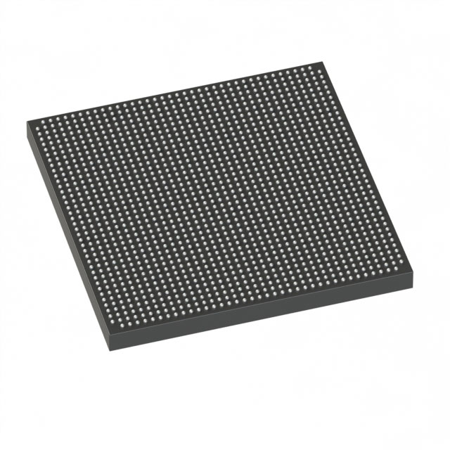
5SGSED8K2F40I3G
| Part Description |
Stratix® V GS Field Programmable Gate Array (FPGA) IC 696 51200000 695000 1517-BBGA, FCBGA |
|---|---|
| Quantity | 961 Available (as of October 8, 2026) |
| Product Category | Field Programmable Gate Array (FPGA) |
|---|---|
| Manufacturer | Intel |
| Manufacturing Status | Active |
| Manufacturer Standard Lead Time | 26 Weeks |
| Datasheet |
Specifications & Environmental
| Device Package | 1517-FBGA (40x40) | Grade | Industrial | Operating Temperature | -40°C – 100°C | ||
|---|---|---|---|---|---|---|---|
| Package / Case | 1517-BBGA, FCBGA | Number of I/O | 696 | Voltage | 820 mV - 880 mV | ||
| Mounting Method | Surface Mount | RoHS Compliance | RoHS Compliant | REACH Compliance | REACH Unaffected | ||
| Moisture Sensitivity Level | 3 (168 Hours) | Number of LABs/CLBs | 262400 | Number of Logic Elements/Cells | 695000 | ||
| Number of Gates | N/A | ECCN | N/A | HTS Code | N/A | ||
| Qualification | N/A | Total RAM Bits | 51200000 |
Overview of 5SGSED8K2F40I3G – Stratix® V GS Field Programmable Gate Array (FPGA)
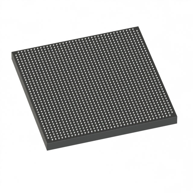
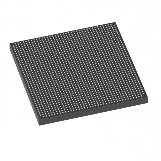
The 5SGSED8K2F40I3G is a Stratix® V GS Field Programmable Gate Array (FPGA) in a 1517-ball FCBGA package, manufactured by Intel. This device delivers very high logic density and extensive I/O connectivity for designs that require large on-chip resources and industrial temperature operation.
With approximately 695,000 logic elements and roughly 51.2 Mbits of embedded memory, the device is targeted at applications that need substantial programmable logic capacity, significant embedded RAM, and a large count of external interfaces.
Key Features
- Core Logic Approximately 695,000 logic elements provide high-density programmable logic for complex digital designs.
- Logic Blocks (LABs/CLBs) 262,400 logic array blocks (LABs/CLBs) to structure and distribute large logic implementations efficiently.
- Embedded Memory Approximately 51.2 Mbits of on-chip RAM to support buffering, caching, and data-path requirements.
- High I/O Count 696 programmable I/O pins for broad connectivity to peripherals, interfaces, and board-level systems.
- Power Supply Core voltage supply range 820 mV to 880 mV to match system power design requirements.
- Package & Mounting 1517-ball BGA (FCBGA) package, supplier package listed as 1517-FBGA (40×40), optimized for surface-mount PCBs.
- Temperature and Grade Industrial grade with an operating temperature range of −40 °C to 100 °C for demanding environments.
- Regulatory RoHS compliant.
Typical Applications
- High-density digital processing Use the large logic element count and abundant on-chip RAM to implement complex state machines, DSP pipelines, and parallel processing engines.
- High I/O connectivity systems Leverage 696 I/O pins to interface with multiple sensors, high-speed boards, and large peripheral arrays.
- Industrial control and automation Industrial temperature rating (−40 °C to 100 °C) and robust packaging make the device suitable for control systems and factory automation equipment requiring stable operation across wide temperatures.
- Board-level subsystem integration Packaged in a 1517-ball FCBGA with surface-mount mounting, the device supports compact, high-density board designs where integration and footprint matter.
Unique Advantages
- Highly scalable logic capacity: Approximately 695,000 logic elements enable designs to scale without partitioning across multiple FPGAs.
- Substantial on-chip memory: Around 51.2 Mbits of embedded RAM reduces dependence on external memory for many buffering and caching tasks.
- Extensive external connectivity: 696 I/O pins allow broad interfacing options for multi-channel and mixed-signal systems.
- Industrial-grade thermal range: Rated from −40 °C to 100 °C for reliable operation in temperature-constrained and outdoor environments.
- Compact, board-ready package: 1517-ball FCBGA (1517-FBGA, 40×40) supports dense PCB layouts and surface-mount assembly.
- Vendor-backed documentation: Supported by Intel Stratix V device documentation for electrical and switching characteristics.
Why Choose 5SGSED8K2F40I3G?
The 5SGSED8K2F40I3G positions itself as a high-density, industrial-grade FPGA option for engineers who need substantial programmable logic, significant embedded memory, and a very high I/O count in a compact FCBGA package. Its combination of approximately 695,000 logic elements, roughly 51.2 Mbits of RAM, and 696 I/Os makes it suitable for complex digital processing, large interface aggregation, and industrial applications requiring extended temperature operation.
Supported by Intel Stratix V device documentation, this device is aimed at designs that value integration density, predictable electrical characteristics, and a package footprint appropriate for space-constrained, high-performance systems.
Request a quote or submit an inquiry to receive pricing and availability information for the 5SGSED8K2F40I3G.





















Date Founded: 1968
Headquarters: Santa Clara, California, USA
Employees: 130,000+
Revenue: $54.23 Billion
Certifications and Memberships: ISO9001:2015, ISO14001:2015, ISO17025:2017, ISO27001:2022, ISO45001:2018, ISO50001:2018


