
5SGSMD5K2F40C3N
| Part Description |
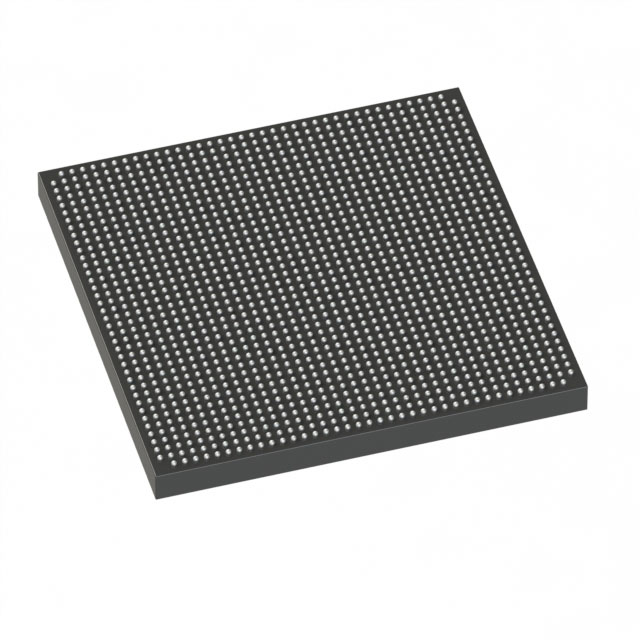
Stratix® V GS Field Programmable Gate Array (FPGA) IC 696 39936000 457000 1517-BBGA, FCBGA |
|---|---|
| Quantity | 1,396 Available (as of June 10, 2026) |

| Product Category | Field Programmable Gate Array (FPGA) |
|---|---|
| Manufacturer | Intel |
| Manufacturing Status | Obsolete |
| Manufacturer Standard Lead Time | Contact Us |
| Datasheet |
Specifications & Environmental
| Device Package | 1517-FBGA (40x40) | Grade | Commercial | Operating Temperature | 0°C – 85°C | ||
|---|---|---|---|---|---|---|---|
| Package / Case | 1517-BBGA, FCBGA | Number of I/O | 696 | Voltage | 820 mV - 880 mV | ||
| Mounting Method | Surface Mount | RoHS Compliance | RoHS Compliant | REACH Compliance | REACH Unknown | ||
| Moisture Sensitivity Level | 3 (168 Hours) | Number of LABs/CLBs | 172600 | Number of Logic Elements/Cells | 457000 | ||
| Number of Gates | N/A | ECCN | 3A001A2C | HTS Code | 8542.39.0001 | ||
| Qualification | N/A | Total RAM Bits | 39936000 |
Overview of 5SGSMD5K2F40C3N – Stratix® V GS FPGA, 457,000 logic elements, ~39.9 Mbits RAM, 696 I/Os, 1517-FBGA
The 5SGSMD5K2F40C3N is a Stratix® V GS field programmable gate array (FPGA) in a 1517-FBGA (40×40) surface-mount package targeted for commercial applications. It combines a high logic capacity fabric with abundant I/O and on-chip memory to address compute- and transceiver-centric designs.
Built on the Stratix V architecture, this GS variant is positioned for transceiver-based, DSP-centric workloads found in wireline, military, broadcast, and high-performance computing applications. Its architecture emphasizes integration of DSP resources, embedded memory, and high-density I/O to support bandwidth- and data-intensive designs.
Key Features
- Core logic 457,000 logic elements provide substantial programmable logic capacity for complex state machines, control, and custom datapaths.
- Embedded memory Approximately 39.9 Mbits of on-chip RAM (39,936,000 bits) using Stratix V M20K memory blocks to support large buffers and scratchpad storage.
- DSP and hard IP Stratix V GS family devices include an abundance of variable-precision DSP blocks; the family supports high-precision multiply resources and integrated hard IP for functions such as PCIe (per the device family documentation).
- I/O and connectivity 696 I/Os enable dense external interfacing and high-pin-count board designs suitable for high-bandwidth systems.
- Package and mounting 1517-FBGA (40×40) FCBGA package in a surface-mount form factor for board-level integration.
- Power supply Core voltage range specified at 820 mV to 880 mV for power planning and system-level thermal design.
- Operating conditions Commercial grade device with an operating temperature range of 0 °C to 85 °C and RoHS compliance.
- Process and architecture Stratix V family devices are implemented in a 28‑nm process and include architecture features such as redesigned adaptive logic modules, multi-track routing, and fabric clocking networks (family-level characteristics).
Typical Applications
- High-performance signal processing Use the device's abundant DSP resources and large on-chip memory for compute-intensive DSP pipelines and real-time data processing.
- Optical and packet transport systems High logic density and many I/Os support complex protocol handling and packet processing in wireline and transport applications.
- Broadcast and military communications The GS variant's DSP and transceiver-focused architecture supports modulation, encoding/decoding, and signal conditioning workloads in broadcast and defense systems.
- System prototyping for ASIC transition Stratix V devices can be used as a low-risk prototyping step with a defined path to HardCopy V ASICs (family-level capability), aiding volume production planning.
Unique Advantages
- High logic and memory integration: 457,000 logic elements paired with approximately 39.9 Mbits of embedded RAM reduce the need for external memory and simplify board design for complex systems.
- Dense I/O for connectivity: 696 I/Os enable rich peripheral and high-speed interface support without extensive multiplexing or external translators.
- Commercial-grade, RoHS-compliant: Designed for commercial temperature ranges (0 °C to 85 °C) and compliant with RoHS requirements for simplified supply-chain compliance.
- Designed for DSP-centric workloads: The GS family’s variable-precision DSP blocks and architecture features provide flexible arithmetic resources for signal-processing applications.
- Proven device family infrastructure: Stratix V family features such as M20K memory blocks, PLLs, and adaptive logic modules support repeatable design patterns and system-level integration.
Why Choose 5SGSMD5K2F40C3N?
The 5SGSMD5K2F40C3N delivers a balanced combination of high logic density, substantial on-chip memory, and a large number of I/Os in a compact 1517-FBGA package—making it suitable for designers targeting DSP-heavy, transceiver-based systems in commercial markets. Its specification set supports complex algorithms, large buffering, and extensive external interfacing while conforming to commercial operating and supply requirements.
For teams planning prototyping and forward migration to ASICs, the Stratix V family provides a documented path to HardCopy V ASICs and a well-established architectural foundation, helping preserve design investment across development and production phases.
Request a quote or submit an inquiry for 5SGSMD5K2F40C3N to check availability and pricing or to discuss how this Stratix V GS device fits your design requirements.


Date Founded: 1968
Headquarters: Santa Clara, California, USA
Employees: 130,000+
Revenue: $54.23 Billion
Certifications and Memberships: ISO9001:2015, ISO14001:2015, ISO17025:2017, ISO27001:2022, ISO45001:2018, ISO50001:2018


