
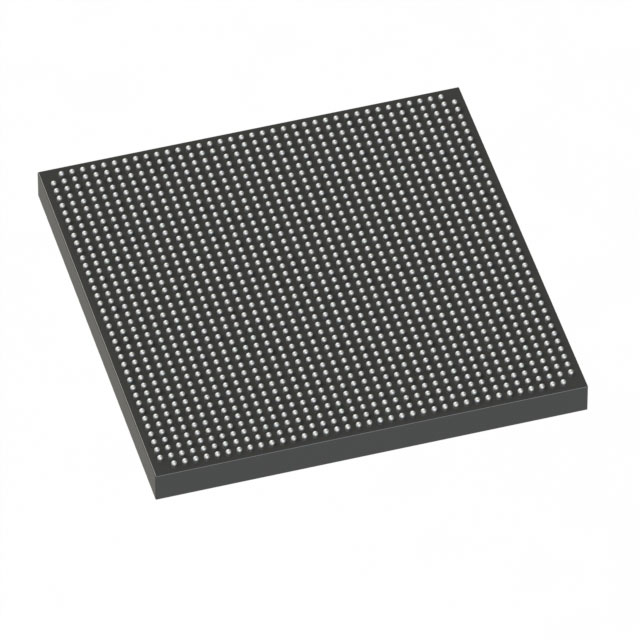
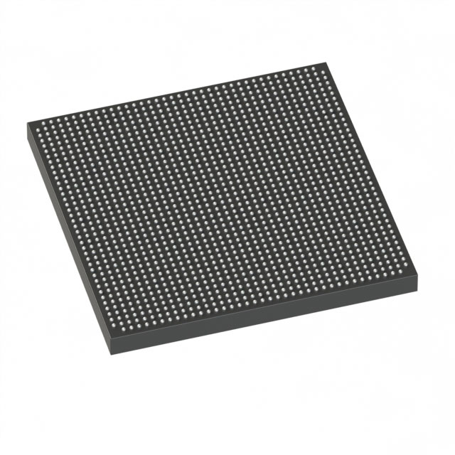
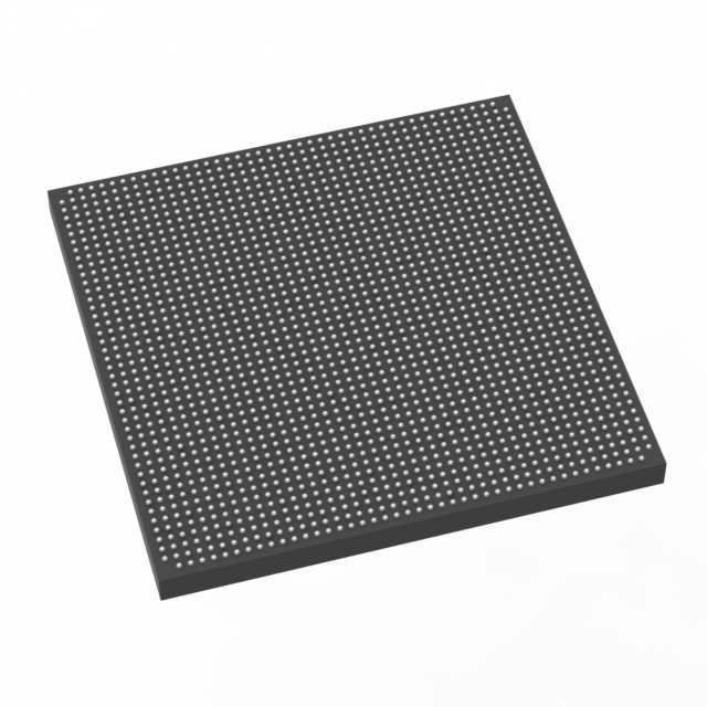
5SGTMC5K2F40C1
| Part Description |
Stratix® V GT Field Programmable Gate Array (FPGA) IC 600 46080000 425000 1517-BBGA, FCBGA |
|---|---|
| Quantity | 996 Available (as of October 8, 2026) |
| Product Category | Field Programmable Gate Array (FPGA) |
|---|---|
| Manufacturer | Intel |
| Manufacturing Status | Obsolete |
| Manufacturer Standard Lead Time | Contact Us |
| Datasheet |
Specifications & Environmental
| Device Package | 1517-FBGA (40x40) | Grade | Commercial | Operating Temperature | 0°C – 85°C | ||
|---|---|---|---|---|---|---|---|
| Package / Case | 1517-BBGA, FCBGA | Number of I/O | 600 | Voltage | 870 mV - 930 mV | ||
| Mounting Method | Surface Mount | RoHS Compliance | Unknown | REACH Compliance | REACH Unknown | ||
| Moisture Sensitivity Level | 3 (168 Hours) | Number of LABs/CLBs | 160500 | Number of Logic Elements/Cells | 425000 | ||
| Number of Gates | N/A | ECCN | OBSOLETE | HTS Code | 0000.00.0000 | ||
| Qualification | N/A | Total RAM Bits | 46080000 |
Overview of 5SGTMC5K2F40C1 – Stratix® V GT FPGA, 425,000 logic elements, 600 I/O
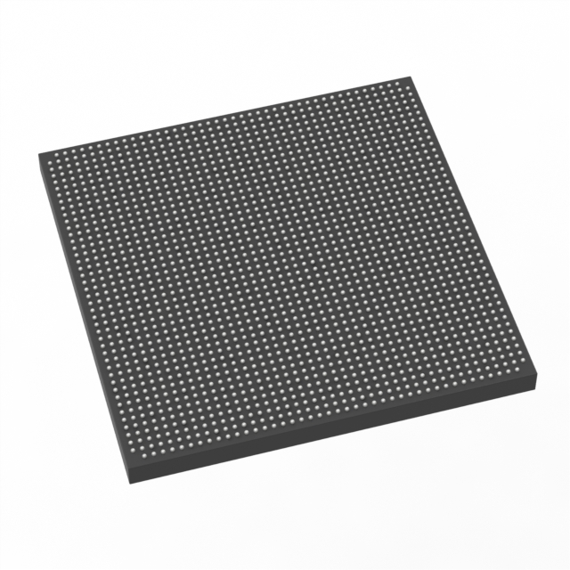
The 5SGTMC5K2F40C1 is a Stratix® V GT Field Programmable Gate Array (FPGA) in a 1517-BBGA (FCBGA) package, offering high logic density and extensive I/O for complex, programmable digital designs. With 425,000 logic elements, approximately 46 Mbits of embedded memory and a large register count, this commercial-grade FPGA targets designs that require substantial on-chip resources and multi-channel interfacing within a commercial temperature range.
Key Features
- Core Logic 425,000 logic elements and 641,600 registers provide a large programmable fabric for complex state machines, control logic and custom datapaths.
- Embedded Memory Approximately 46 Mbits of on-chip RAM to support large buffering, lookup tables and memory-intensive algorithms.
- DSP Resources 256 hardened single-precision floating-point multipliers/adders and 256 18×18 multipliers for high-throughput signal and numeric processing.
- Clocking and Timing 16 global clocks, 92 regional clocks and 28 PLLs to support flexible clock domain partitioning and multi-rate designs.
- I/O and Channel Density 600 GPIO pins provide broad external interfacing capability; datasheet specifies support for up to 150 LVDS channels.
- Package and Mounting 1517-BBGA (FCBGA) package, supplier device package listed as 1517-FBGA (40×40), and surface-mount mounting for high-density board integration.
- Power and Supply Specified core voltage range of 870 mV to 930 mV to align with board-level power delivery planning.
- Operating Conditions & Compliance Commercial grade operation from 0 °C to 85 °C and RoHS compliance for regulatory alignment.
Typical Applications
- High-performance signal processing Use the 256 DSP multipliers and substantial on-chip RAM to implement pipelines for filtering, transforms and real-time numeric workloads.
- Multi-channel data aggregation Leverage 600 I/O and abundant clocking resources to consolidate and route data from many parallel sources.
- Complex control systems Large logic element and register counts enable sophisticated control, sequencing and state-machine implementations for embedded systems.
- Prototype and system integration The high logic density and flexible IO make this device suitable for consolidating multiple functions onto a single FPGA for evaluation or integration.
Unique Advantages
- High logic capacity: 425,000 logic elements allow large-scale integration of functions that reduce external component count and simplify board-level design.
- Substantial on-chip memory: Approximately 46 Mbits of embedded RAM supports buffering and local data storage, reducing reliance on external memory.
- Robust DSP capabilities: 256 floating-point and 18×18 multipliers accelerate compute-heavy algorithms, shortening development of signal-processing blocks.
- Flexible clocking fabric: Multiple global and regional clocks plus 28 PLLs provide timing flexibility for multi-domain systems and mixed-rate interfaces.
- High I/O count in compact package: 600 GPIO in a 1517-BBGA FCBGA footprint supports dense I/O routing while maintaining a compact PCB footprint.
- Commercial-temperature readiness: Rated for 0 °C to 85 °C operation and RoHS compliant for use in standard commercial deployments.
Why Choose 5SGTMC5K2F40C1?
The 5SGTMC5K2F40C1 positions itself as a high-density, DSP-forward Stratix® V GT FPGA tailored for designs that require extensive programmable logic, on-chip memory and a large I/O complement within a commercial temperature range. Its combination of 425,000 logic elements, approximately 46 Mbits of embedded RAM, and 256 hardware multipliers makes it well suited for developers consolidating complex digital, control and signal-processing functions onto a single device.
For teams building multi-channel data systems, high-throughput processing blocks, or dense integration prototypes, this FPGA offers a balance of resources and package density to help reduce external components and streamline system architecture planning.
Request a quote or submit a procurement inquiry to receive pricing and availability information for the 5SGTMC5K2F40C1. Technical and ordering support can assist with part selection and delivery timelines.





















Date Founded: 1968
Headquarters: Santa Clara, California, USA
Employees: 130,000+
Revenue: $54.23 Billion
Certifications and Memberships: ISO9001:2015, ISO14001:2015, ISO17025:2017, ISO27001:2022, ISO45001:2018, ISO50001:2018


