
5SGXEA5N2F40I3LN
| Part Description |
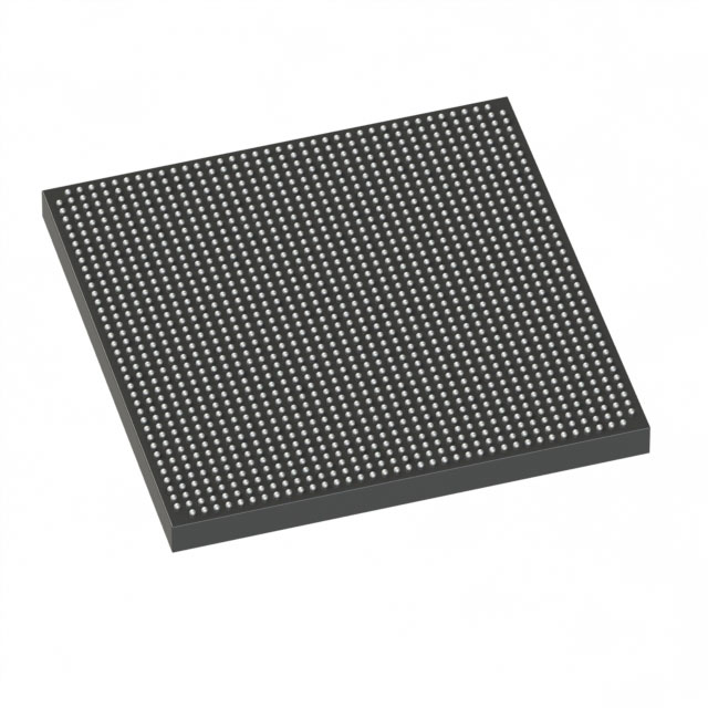
Stratix® V GX Field Programmable Gate Array (FPGA) IC 600 46080000 490000 1517-BBGA, FCBGA |
|---|---|
| Quantity | 248 Available (as of June 10, 2026) |
| Product Category | Field Programmable Gate Array (FPGA) |
|---|---|
| Manufacturer | Intel |
| Manufacturing Status | Obsolete |
| Manufacturer Standard Lead Time | Contact Us |
| Datasheet |
Specifications & Environmental
| Device Package | 1517-FBGA (40x40) | Grade | Industrial | Operating Temperature | -40°C – 100°C | ||
|---|---|---|---|---|---|---|---|
| Package / Case | 1517-BBGA, FCBGA | Number of I/O | 600 | Voltage | 820 mV - 880 mV | ||
| Mounting Method | Surface Mount | RoHS Compliance | RoHS Compliant | REACH Compliance | REACH Unknown | ||
| Moisture Sensitivity Level | 3 (168 Hours) | Number of LABs/CLBs | 185000 | Number of Logic Elements/Cells | 490000 | ||
| Number of Gates | N/A | ECCN | 3A001A2C | HTS Code | 8542.39.0001 | ||
| Qualification | N/A | Total RAM Bits | 46080000 |
Overview of 5SGXEA5N2F40I3LN – Stratix® V GX FPGA, 490,000 Logic Elements, 1517-BBGA
The 5SGXEA5N2F40I3LN is a Stratix V GX field-programmable gate array (FPGA) designed for high-density programmable logic applications. It combines 490,000 logic elements with approximately 46 Mbits of embedded memory and up to 600 I/O pins to address complex, memory- and I/O-intensive designs in industrial environments.
As a member of the Stratix V GX family, the device is offered within the series’ documented transceiver speed-grade options and electrical characteristics, enabling designers to target high-bandwidth serial interfaces and large-scale system integration where high logic density and extensive I/O are required.
Key Features
- Logic Capacity 490,000 logic elements for implementing large, complex FPGA designs and extensive custom logic.
- Embedded Memory Approximately 46 Mbits of on-chip RAM to support buffering, packet processing, and large lookup tables without external memory for many functions.
- I/O Count Up to 600 user I/O pins provides broad interfacing capability for high-pin-count systems, mezzanine connections, and multi-protocol designs.
- Power and Core Voltage Core supply range specified at 820 mV to 880 mV for devices manufactured to the Stratix V electrical characteristics.
- Package & Mounting 1517-BBGA (FCBGA) supplier package, 1517-FBGA (40×40) footprint; surface-mount mounting type suited for board-level assembly.
- Industrial Temperature Grade Rated for operation from –40 °C to 100 °C and specified as Industrial grade for temperature-sensitive deployments.
- Standards & Compliance RoHS-compliant, meeting requirements for restricted substances in electronic assemblies.
- Stratix V GX Family Capabilities Stratix V GX devices are documented with multiple transceiver speed grades in the device datasheet, supporting a range of high-speed serial channel options across the family.
Typical Applications
- High-bandwidth packet processing Large logic capacity and abundant on-chip RAM allow implementation of packet engines, traffic managers, and protocol offloads without relying solely on external memory.
- High-speed serial communications As part of the Stratix V GX family, the device aligns with family-level transceiver speed-grade offerings for demanding serial link and backplane interfaces.
- Complex control and instrumentation Industrial temperature rating and extensive I/O make it suitable for control systems, data acquisition, and instrumentation requiring robust operation across wide temperature ranges.
- Prototyping and SoC integration High logic element count and embedded memory facilitate system prototyping and acceleration of compute-intensive functions within mixed hardware/software solutions.
Unique Advantages
- High logic density: 490,000 logic elements enable large-scale custom hardware implementations and complex state machines without partitioning across multiple devices.
- Significant on-chip RAM: Approximately 46 Mbits of embedded memory reduces dependency on external DRAM for many buffering and storage needs, simplifying board design.
- Extensive I/O: 600 I/Os provide flexibility for multi-lane interfaces, wide parallel buses, and rich peripheral connectivity directly from the FPGA package.
- Industrial readiness: Rated –40 °C to 100 °C and designated Industrial grade to meet the thermal and reliability needs of industrial deployments.
- Compact, industry-standard package: 1517-BBGA (40×40) FCBGA package enables high pin count in a compact surface-mount footprint compatible with standard assembly processes.
- Regulatory compliance: RoHS compliance supports use in assemblies where restricted substance requirements apply.
Why Choose 5SGXEA5N2F40I3LN?
The 5SGXEA5N2F40I3LN positions itself as a high-density Stratix V GX FPGA option for engineers needing substantial programmable logic, large embedded RAM, and a high I/O count in an industrial-grade package. Its documented Stratix V family characteristics provide guidance for designers targeting high-speed serial interfaces and large system integration tasks.
This device is suitable for design teams developing complex data-paths, protocol engines, and control systems that require on-chip memory and plentiful I/O while operating across a wide industrial temperature range. The combination of logic capacity, memory, and packaging supports scalable designs and long-term deployment in demanding environments.
Request a quote or submit a sales inquiry to obtain pricing, availability, and technical support for the 5SGXEA5N2F40I3LN.


Date Founded: 1968
Headquarters: Santa Clara, California, USA
Employees: 130,000+
Revenue: $54.23 Billion
Certifications and Memberships: ISO9001:2015, ISO14001:2015, ISO17025:2017, ISO27001:2022, ISO45001:2018, ISO50001:2018


