
5SGXEA7K3F40C2G
| Part Description |
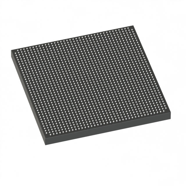
Stratix® V GX Field Programmable Gate Array (FPGA) IC 696 51200000 622000 1517-BBGA, FCBGA |
|---|---|
| Quantity | 347 Available (as of June 18, 2026) |

| Product Category | Field Programmable Gate Array (FPGA) |
|---|---|
| Manufacturer | Intel |
| Manufacturing Status | Active |
| Manufacturer Standard Lead Time | 26 Weeks |
| Datasheet |
Specifications & Environmental
| Device Package | 1517-FBGA (40x40) | Grade | Commercial | Operating Temperature | 0°C – 85°C | ||
|---|---|---|---|---|---|---|---|
| Package / Case | 1517-BBGA, FCBGA | Number of I/O | 696 | Voltage | 870 mV - 930 mV | ||
| Mounting Method | Surface Mount | RoHS Compliance | RoHS Compliant | REACH Compliance | REACH Unaffected | ||
| Moisture Sensitivity Level | 3 (168 Hours) | Number of LABs/CLBs | 234720 | Number of Logic Elements/Cells | 622000 | ||
| Number of Gates | N/A | ECCN | N/A | HTS Code | N/A | ||
| Qualification | N/A | Total RAM Bits | 51200000 |
Overview of 5SGXEA7K3F40C2G – Stratix® V GX Field Programmable Gate Array (FPGA) IC
The 5SGXEA7K3F40C2G is a Stratix V GX family FPGA from Intel, delivered in a 1517-BBGA FCBGA package. It provides high on-chip logic and memory capacity with extensive I/O and is offered in a commercial temperature grade for general-purpose embedded and programmable logic applications.
With a large logic element count and substantial embedded RAM, this device targets designs that require dense programmable logic, significant on-chip storage, and a high I/O pin count while operating within standard commercial temperature and supply ranges.
Key Features
- Logic Capacity Approximately 622,000 logic elements for implementing complex, high-density logic designs.
- Embedded Memory Approximately 51.2 Mbits of on-chip RAM to support large buffering, state machines, and data-path storage.
- I/O Resources 696 general-purpose I/O pins to support broad interfacing with external devices and high pin-count systems.
- Power and Core Supply Core voltage supply range of 870 mV to 930 mV to match system power-rail requirements for this device.
- Package and Mounting Supplied in a 1517-BBGA FCBGA package (supplier device package: 1517-FBGA, 40×40); surface-mount mounting type for PCB integration.
- Temperature Grade Commercial operating temperature range: 0 °C to 85 °C.
- Standards Compliance RoHS compliant.
Typical Applications
- High-density programmable systems Leverage ~622,000 logic elements and ~51.2 Mbits of embedded memory to implement sizable custom logic and datapath functions on a single device.
- Data buffering and on-chip storage Use the substantial embedded RAM for large FIFOs, packet buffering, and intermediate storage in data-path applications.
- High-pin-count interfaces Take advantage of 696 I/Os to connect to multiple peripherals, memory interfaces, or distributed I/O requirements on complex PCBs.
Unique Advantages
- High integration density: Combine hundreds of thousands of logic elements with tens of megabits of embedded RAM to reduce board-level component count.
- Extensive I/O capacity: 696 I/Os enable flexible system partitioning and support for multi-channel external interfaces without resorting to additional I/O expanders.
- Commercial-temperature operation: Rated for 0 °C to 85 °C, suitable for standard embedded and commercial applications.
- RoHS compliant: Conforms to RoHS requirements for environmentally conscious manufacturing and supply-chain compatibility.
- Surface-mount package: 1517-BBGA (supplier 1517-FBGA, 40×40) offers a compact footprint for high-density PCB layouts.
- Defined core supply window: 870 mV to 930 mV core supply range supports predictable power planning and thermal management in system design.
Why Choose 5SGXEA7K3F40C2G?
The 5SGXEA7K3F40C2G delivers a balance of large programmable logic capacity, substantial embedded memory, and a high I/O count in a compact surface-mount FCBGA package. Its commercial temperature rating and RoHS compliance make it suitable for a wide range of standard embedded designs that require dense on-chip resources and extensive external connectivity.
Backed by Intel’s Stratix V device documentation, this FPGA is appropriate for engineering teams building complex, high-density programmable logic solutions that demand integrated memory, many I/Os, and a clearly defined core power envelope for system-level power and thermal planning.
Request a quote or submit an inquiry to purchase or evaluate 5SGXEA7K3F40C2G for your next high-density FPGA design project.


Date Founded: 1968
Headquarters: Santa Clara, California, USA
Employees: 130,000+
Revenue: $54.23 Billion
Certifications and Memberships: ISO9001:2015, ISO14001:2015, ISO17025:2017, ISO27001:2022, ISO45001:2018, ISO50001:2018


