
5SGXMA7K1F40I2G
| Part Description |
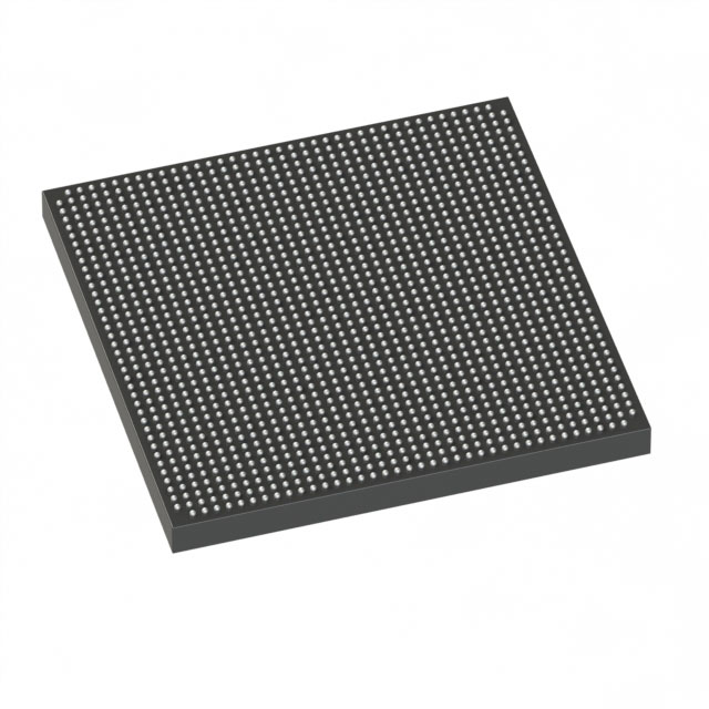
Stratix® V GX Field Programmable Gate Array (FPGA) IC 696 51200000 622000 1517-BBGA, FCBGA |
|---|---|
| Quantity | 1,536 Available (as of June 14, 2026) |

| Product Category | Field Programmable Gate Array (FPGA) |
|---|---|
| Manufacturer | Intel |
| Manufacturing Status | Active |
| Manufacturer Standard Lead Time | 26 Weeks |
| Datasheet |
Specifications & Environmental
| Device Package | 1517-FBGA (40x40) | Grade | Industrial | Operating Temperature | -40°C – 100°C | ||
|---|---|---|---|---|---|---|---|
| Package / Case | 1517-BBGA, FCBGA | Number of I/O | 696 | Voltage | 870 mV - 930 mV | ||
| Mounting Method | Surface Mount | RoHS Compliance | RoHS Compliant | REACH Compliance | REACH Unaffected | ||
| Moisture Sensitivity Level | 3 (168 Hours) | Number of LABs/CLBs | 234720 | Number of Logic Elements/Cells | 622000 | ||
| Number of Gates | N/A | ECCN | N/A | HTS Code | N/A | ||
| Qualification | N/A | Total RAM Bits | 51200000 |
Overview of 5SGXMA7K1F40I2G – Stratix® V GX Field Programmable Gate Array (FPGA), 1517-BBGA FCBGA
The 5SGXMA7K1F40I2G is a Stratix® V GX Field Programmable Gate Array (FPGA) IC optimized for high-density programmable logic applications. It provides a large on-chip programmable fabric with substantial embedded memory, a high I/O count, and industrial-grade operating range for designs that require extended temperature tolerance and robust integration.
This device targets designs that need significant logic resources, abundant I/O, and a low-voltage core operating window, enabling compact, high-functionality implementations in industrial and communications-focused equipment.
Key Features
- High-density logic — 622,000 logic elements (cells) to implement complex digital designs and large-scale FPGA functions.
- Embedded memory — approximately 51.2 Mbits of on-chip RAM to support buffers, FIFOs, and on-chip data storage for performance-critical designs.
- Rich I/O — 696 I/O pins to accommodate complex board-level interfaces and high pin-count system integration.
- Power and core voltage — core voltage supply range of 870 mV to 930 mV for low-voltage core operation.
- Industrial temperature grade — specified operating temperature from −40 °C to 100 °C for deployments in industrial environments.
- Package and mounting — 1517-BBGA (FCBGA) package, supplier package listed as 1517-FBGA (40×40), surface-mount mounting for high-density PCB integration.
- Compliance — RoHS-compliant manufacturing to meet environmental and regulatory requirements.
Typical Applications
- High-density digital systems — Implement complex logic, custom accelerators, and protocol handling using the device’s large logic element count and embedded memory.
- Communications and networking equipment — Leverage the high I/O count and large programmable fabric for packet processing, protocol bridging, and interface aggregation.
- Industrial control and automation — Use industrial temperature range and abundant I/O for reliable control, signal aggregation, and real-time processing in industrial environments.
Unique Advantages
- Large programmable fabric: 622,000 logic elements enable consolidation of multiple functions into a single device, reducing board-level BOM and interfaces.
- Significant on-chip memory: Approximately 51.2 Mbits of embedded RAM supports data buffering and on-chip acceleration without extensive external memory.
- High I/O density: 696 I/Os provide flexibility to connect to numerous peripherals, transceivers, and system interfaces directly at the FPGA.
- Industrial-grade thermal range: Rated from −40 °C to 100 °C for deployments where extended temperature tolerance is required.
- Compact, surface-mount packaging: 1517-BBGA FCBGA package supports high-density PCB designs while maintaining robust mechanical and thermal characteristics.
- Environmentally compliant: RoHS status ensures the device meets common environmental compliance needs.
Why Choose 5SGXMA7K1F40I2G?
The 5SGXMA7K1F40I2G delivers a balance of extensive logic resources, substantial embedded memory, and a high I/O count in a single, industrial-grade FCBGA package. Its low-voltage core operating window and surface-mount BBGA footprint enable compact, power-aware designs while supporting demanding integration requirements.
This device is well suited to engineering teams building complex digital systems, communications equipment, or industrial control platforms that require on-chip capacity for logic and memory, high interface density, and reliable operation across an extended temperature range.
Request a quote or submit an inquiry to initiate procurement or obtain pricing and availability information for the 5SGXMA7K1F40I2G.


Date Founded: 1968
Headquarters: Santa Clara, California, USA
Employees: 130,000+
Revenue: $54.23 Billion
Certifications and Memberships: ISO9001:2015, ISO14001:2015, ISO17025:2017, ISO27001:2022, ISO45001:2018, ISO50001:2018


