
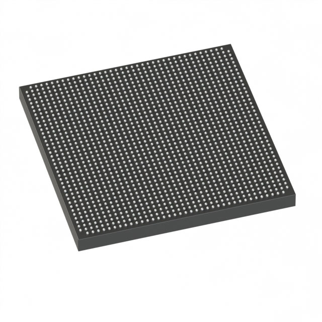
5SGXMA7K1F40C2WN
| Part Description |
Stratix® V GX Field Programmable Gate Array (FPGA) IC 696 51200000 622000 1517-BBGA, FCBGA |
|---|---|
| Quantity | 378 Available (as of June 10, 2026) |

| Product Category | Field Programmable Gate Array (FPGA) |
|---|---|
| Manufacturer | Intel |
| Manufacturing Status | Obsolete |
| Manufacturer Standard Lead Time | Contact Us |
| Datasheet |
Specifications & Environmental
| Device Package | 1517-FBGA (40x40) | Grade | Commercial | Operating Temperature | 0°C – 85°C | ||
|---|---|---|---|---|---|---|---|
| Package / Case | 1517-BBGA, FCBGA | Number of I/O | 696 | Voltage | 870 mV - 930 mV | ||
| Mounting Method | Surface Mount | RoHS Compliance | RoHS non-compliant | REACH Compliance | REACH Unknown | ||
| Moisture Sensitivity Level | 4 (72 Hours) | Number of LABs/CLBs | 234720 | Number of Logic Elements/Cells | 622000 | ||
| Number of Gates | N/A | ECCN | OBSOLETE | HTS Code | N/A | ||
| Qualification | N/A | Total RAM Bits | 51200000 |
Overview of 5SGXMA7K1F40C2WN – Stratix® V GX FPGA, 622,000 logic elements, ~51.2 Mbits RAM, 696 I/Os, 1517-FBGA (40×40)
The 5SGXMA7K1F40C2WN is a Stratix V GX field programmable gate array (FPGA) in a 1517-ball FCBGA package. It provides a high-density programmable fabric with 622,000 logic elements and approximately 51.2 Mbits of embedded RAM, delivered in a commercial-grade FPGA rated for 0 °C to 85 °C operation.
Engineered for applications that require substantial logic capacity and large on-chip memory, this device offers extensive I/O (696 pins), surface-mount packaging, and a documented Stratix V device architecture with transceiver and I/O timing details available in the device datasheet.
Key Features
- Core Logic 622,000 logic elements provide large programmable fabric for complex digital designs.
- Embedded Memory Approximately 51.2 Mbits of on-chip RAM for buffering, tables, and fast local storage.
- I/O Capacity 696 I/O pins to support extensive peripheral, bus, and board-level connectivity.
- Package and Mounting 1517-BBGA / 1517-FBGA (40×40) FCBGA package in a surface-mount form factor for dense board layouts.
- Power and Operating Range Core supply range specified at 870 mV to 930 mV with an ambient operating temperature range of 0 °C to 85 °C (commercial grade).
- Series-Level Transceiver Information Stratix V GX family documentation includes transceiver and I/O timing specifications; the series lists GX channel transceiver speed grades up to 14.1 Gbps (refer to the Stratix V device documentation for details).
- Regulatory RoHS compliant.
Unique Advantages
- High logic density: 622,000 logic elements enable implementation of large, complex FPGA designs without partitioning across multiple devices.
- Substantial on-chip memory: Approximately 51.2 Mbits of embedded RAM reduce external memory requirements and improve data-path performance.
- Extensive I/O: 696 I/Os allow flexible interfacing to multiple peripherals, high-pin-count buses, and board-level routing options.
- Compact FCBGA package: The 1517-ball FCBGA (40×40) provides a dense package footprint suitable for space-constrained PCBs while supporting high I/O counts.
- Commercial operating range: Rated for 0 °C to 85 °C, aligning with commercial deployment requirements.
- Documented device architecture: Full Stratix V device datasheet details core, transceiver, and I/O electrical characteristics for design and validation.
Why Choose 5SGXMA7K1F40C2WN?
This Stratix V GX FPGA delivers a combination of high logic capacity, large embedded memory, and broad I/O in a compact FCBGA package for commercial applications. It is designed for engineering teams who need substantial on-chip resources and documented electrical and timing characteristics from the Stratix V family to support system-level integration and verification.
Choosing this device allows you to consolidate complex functions into a single high-density FPGA, simplify board-level routing with plentiful I/Os, and leverage the Stratix V documentation for design and power planning.
If you would like pricing, availability, or a formal quote for the 5SGXMA7K1F40C2WN, request a quote or submit an inquiry to receive sales and ordering information.


Date Founded: 1968
Headquarters: Santa Clara, California, USA
Employees: 130,000+
Revenue: $54.23 Billion
Certifications and Memberships: ISO9001:2015, ISO14001:2015, ISO17025:2017, ISO27001:2022, ISO45001:2018, ISO50001:2018


