
5SGXMA7K1F40C2G
| Part Description |
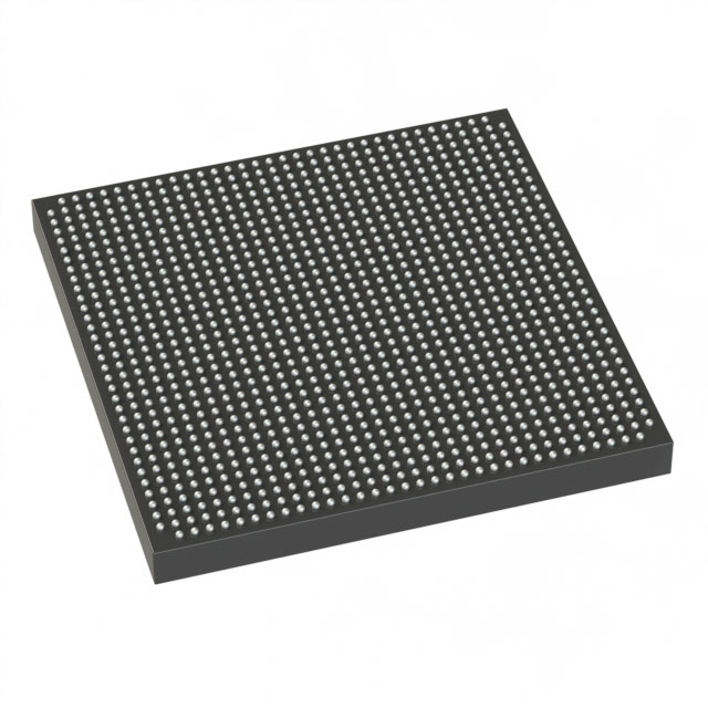
Stratix® V GX Field Programmable Gate Array (FPGA) IC 696 51200000 622000 1517-BBGA, FCBGA |
|---|---|
| Quantity | 528 Available (as of June 15, 2026) |

| Product Category | Field Programmable Gate Array (FPGA) |
|---|---|
| Manufacturer | Intel |
| Manufacturing Status | Active |
| Manufacturer Standard Lead Time | 26 Weeks |
| Datasheet |
Specifications & Environmental
| Device Package | 1517-FBGA (40x40) | Grade | Commercial | Operating Temperature | 0°C – 85°C | ||
|---|---|---|---|---|---|---|---|
| Package / Case | 1517-BBGA, FCBGA | Number of I/O | 696 | Voltage | 870 mV - 930 mV | ||
| Mounting Method | Surface Mount | RoHS Compliance | RoHS Compliant | REACH Compliance | REACH Unaffected | ||
| Moisture Sensitivity Level | 3 (168 Hours) | Number of LABs/CLBs | 234720 | Number of Logic Elements/Cells | 622000 | ||
| Number of Gates | N/A | ECCN | N/A | HTS Code | N/A | ||
| Qualification | N/A | Total RAM Bits | 51200000 |
Overview of 5SGXMA7K1F40C2G – Stratix® V GX Field Programmable Gate Array (FPGA) IC, 622,000 logic elements
The 5SGXMA7K1F40C2G is an Intel Stratix® V GX family FPGA supplied in a 1517-BBGA (1517-FBGA, 40×40) surface-mount package. It delivers very high logic capacity and substantial on-chip memory for complex digital designs that require extensive logic fabric and dense I/O.
This commercial-grade device targets applications that demand large numbers of logic elements, significant embedded RAM, and a high pin-count interface, while operating within a core voltage range of 870 mV to 930 mV and a temperature range of 0 °C to 85 °C.
Key Features
- Core Logic Provides 622,000 logic elements suitable for large-scale programmable logic implementations and complex system integration.
- Embedded Memory Approximately 51.2 Mbits of on-chip RAM to support deep buffering, large data structures, and memory-intensive algorithms.
- I/O Capacity 696 user I/O pins to accommodate high pin-count interfaces and complex board-level connectivity.
- Package & Mounting 1517-BBGA package (supplier package: 1517-FBGA, 40×40) with surface-mount construction for dense system layouts.
- Power Core voltage supply specified between 870 mV and 930 mV to match system power domains and regulator designs.
- Temperature & Grade Commercial grade operation across 0 °C to 85 °C for standard commercial applications.
- Compliance RoHS-compliant for restricted substances and environmental conformity.
- Stratix V GX Family Characteristics As a Stratix V GX device, the family documentation describes high-performance transceiver speed grade options and electrical/switching characteristic guidance.
Typical Applications
- High-density digital systems Large logic capacity and extensive embedded RAM enable integration of complex RTL, hardware accelerators, and multi-module designs on a single device.
- High-pin-count interface systems With 696 I/O pins and a dense BGA package, the device is well-suited to boards requiring numerous external interfaces and parallel buses.
- Memory-intensive processing Approximately 51.2 Mbits of on-chip RAM supports buffering, packet buffering, and local data storage for signal processing or data-path pipelines.
Unique Advantages
- Very high logic capacity: 622,000 logic elements provide the headroom to implement large-scale programmable logic and integrate multiple functions into one FPGA.
- Substantial on-chip memory: Approximately 51.2 Mbits of embedded RAM reduces dependency on external memory for many data-heavy functions.
- Extensive I/O count: 696 I/O pins support complex peripheral and board-level interfacing without additional I/O-expansion components.
- Dense, manufacturable package: The 1517-BBGA (1517-FBGA, 40×40) surface-mount package enables compact board layouts and reliable soldered connections for volume production.
- Commercial temperature operation: Rated for 0 °C to 85 °C to match a wide range of commercial electronic products and systems.
- Environmentally compliant: RoHS compliance supports regulatory and customer requirements for restricted substances.
Why Choose 5SGXMA7K1F40C2G?
This Stratix V GX device combines one of the family’s large logic fabrics with substantial embedded memory and a high I/O count in a compact BGA package, making it a strong fit for designers who need to consolidate complex functions onto a single FPGA. Its electrical characteristics and family documentation provide the guidance required for power, timing, and transceiver considerations when selecting a high-density Stratix V GX solution.
Choose 5SGXMA7K1F40C2G for commercial applications that require significant logic resources, on-chip RAM, and extensive external connectivity while remaining within standard commercial operating and power specifications.
Request a quote or submit a pricing and availability inquiry to evaluate 5SGXMA7K1F40C2G for your next design.


Date Founded: 1968
Headquarters: Santa Clara, California, USA
Employees: 130,000+
Revenue: $54.23 Billion
Certifications and Memberships: ISO9001:2015, ISO14001:2015, ISO17025:2017, ISO27001:2022, ISO45001:2018, ISO50001:2018


