
5SGXMA7K1F40C1WN
| Part Description |
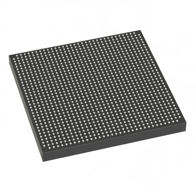
Stratix® V GX Field Programmable Gate Array (FPGA) IC 696 51200000 622000 1517-BBGA, FCBGA |
|---|---|
| Quantity | 803 Available (as of June 18, 2026) |

| Product Category | Field Programmable Gate Array (FPGA) |
|---|---|
| Manufacturer | Intel |
| Manufacturing Status | Obsolete |
| Manufacturer Standard Lead Time | Contact Us |
| Datasheet |
Specifications & Environmental
| Device Package | 1517-FBGA (40x40) | Grade | Commercial | Operating Temperature | 0°C – 85°C | ||
|---|---|---|---|---|---|---|---|
| Package / Case | 1517-BBGA, FCBGA | Number of I/O | 696 | Voltage | 870 mV - 930 mV | ||
| Mounting Method | Surface Mount | RoHS Compliance | RoHS non-compliant | REACH Compliance | REACH Unknown | ||
| Moisture Sensitivity Level | 4 (72 Hours) | Number of LABs/CLBs | 234720 | Number of Logic Elements/Cells | 622000 | ||
| Number of Gates | N/A | ECCN | OBSOLETE | HTS Code | N/A | ||
| Qualification | N/A | Total RAM Bits | 51200000 |
Overview of 5SGXMA7K1F40C1WN – Stratix® V GX FPGA (696 I/Os, 1517‑BBGA)
The 5SGXMA7K1F40C1WN is a Stratix® V GX field‑programmable gate array (FPGA) IC offering very large logic capacity and a high I/O count in a 1517‑ball FCBGA package. With 622,000 logic elements and approximately 51.2 Mbits of embedded RAM, this commercial‑grade device is suited for designs that require substantial on‑chip logic, memory, and dense I/O integration.
Designed for surface‑mount applications, the device operates over a commercial temperature range (0 °C to 85 °C) and supports a nominal core supply window between 870 mV and 930 mV, providing predictable electrical operating conditions for complex digital systems.
Key Features
- High Logic Capacity — 622,000 logic elements to implement large-scale digital designs, custom accelerators, or complex state machines.
- Embedded Memory — Approximately 51.2 Mbits of on‑chip RAM for buffering, packet queues, and large shared memory structures without external DRAM.
- Extensive I/O — 696 user I/Os enabling dense interfacing to high‑pin‑count boards, mezzanines, or multi‑lane peripherals.
- Package & Mounting — 1517‑BBGA (FCBGA) surface‑mount package; supplier package listed as 1517‑FBGA (40×40) for compact, high‑pin‑count PCB designs.
- Power Supply Range — Core supply specified from 870 mV to 930 mV to support regulated core voltage domains and power planning.
- Commercial Temperature Grade — Rated for 0 °C to 85 °C operation for standard commercial applications.
- RoHS Compliant — Conforms to RoHS directives for lead‑free assembly and environmental requirements.
Typical Applications
- High‑density digital processing — Implement complex logic, datapaths, and custom compute functions using the device’s large logic and memory resources.
- Network and telecom infrastructure — Use the high I/O count and on‑chip RAM for packet processing, buffering, and protocol handling in communication equipment.
- Prototyping and system integration — Integrate large IP blocks and system functions on a single FPGA for rapid validation and proof‑of‑concept platforms.
- Custom accelerator boards — Deploy the device where dense logic and local memory improve throughput for application‑specific acceleration tasks.
Unique Advantages
- Substantial on‑chip resources: 622,000 logic elements and ~51.2 Mbits of RAM reduce dependence on external components and simplify board routing.
- High I/O density: 696 I/Os support complex, multi‑lane interfaces and rich peripheral connectivity without multi‑chip solutions.
- Compact, manufacturable package: 1517‑BBGA FCBGA (1517‑FBGA 40×40) enables high pin density in a PCB‑friendly form factor for surface‑mount assembly.
- Predictable electrical envelope: Defined core supply range (870 mV–930 mV) supports consistent power budgeting and regulator selection.
- Commercial readiness: Rated for 0 °C to 85 °C operation and RoHS compliant for mainstream electronic products.
Why Choose 5SGXMA7K1F40C1WN?
The 5SGXMA7K1F40C1WN positions itself as a high‑capacity FPGA option for engineers who need abundant logic, embedded memory, and large I/O capability in a single device. Its combination of 622,000 logic elements, approximately 51.2 Mbits of RAM, and 696 I/Os makes it a practical choice for complex digital systems, network equipment, and custom accelerator designs where integration and density matter.
Backed by Stratix V GX family documentation and designed for surface‑mount assembly in a 1517‑ball FCBGA package, this device is intended for commercial applications that require robust on‑chip resources and clear electrical operating parameters for power and thermal planning.
Request a quote or submit an inquiry to check pricing, availability, and lead times for the 5SGXMA7K1F40C1WN. Provide your quantity and timeline to receive a prompt response for procurement and design planning.


Date Founded: 1968
Headquarters: Santa Clara, California, USA
Employees: 130,000+
Revenue: $54.23 Billion
Certifications and Memberships: ISO9001:2015, ISO14001:2015, ISO17025:2017, ISO27001:2022, ISO45001:2018, ISO50001:2018


