
5SGXMA7K1F35I2WN
| Part Description |
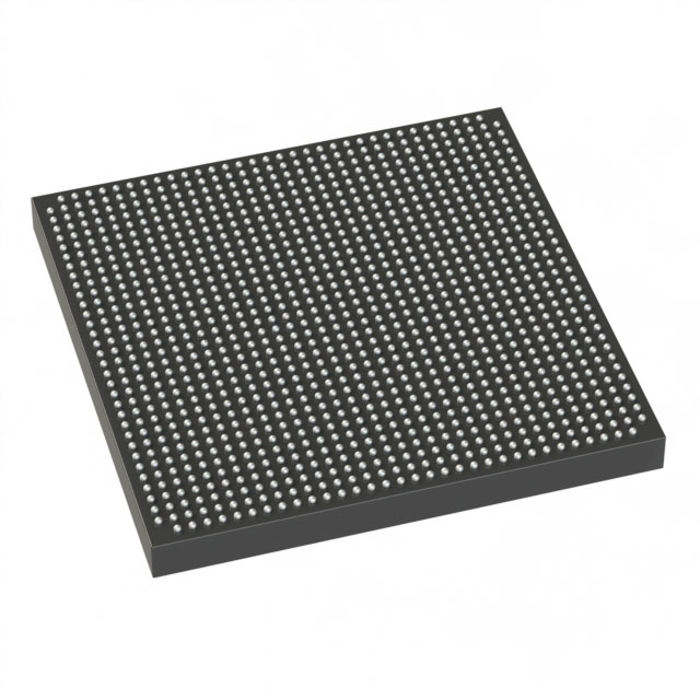
Stratix® V GX Field Programmable Gate Array (FPGA) IC 432 51200000 622000 1152-BBGA, FCBGA |
|---|---|
| Quantity | 734 Available (as of June 18, 2026) |
| Product Category | Field Programmable Gate Array (FPGA) |
|---|---|
| Manufacturer | Intel |
| Manufacturing Status | Obsolete |
| Manufacturer Standard Lead Time | Contact Us |
| Datasheet |
Specifications & Environmental
| Device Package | 1152-FBGA (35x35) | Grade | Industrial | Operating Temperature | -40°C – 100°C | ||
|---|---|---|---|---|---|---|---|
| Package / Case | 1152-BBGA, FCBGA | Number of I/O | 432 | Voltage | 870 mV - 930 mV | ||
| Mounting Method | Surface Mount | RoHS Compliance | RoHS non-compliant | REACH Compliance | REACH Unknown | ||
| Moisture Sensitivity Level | 4 (72 Hours) | Number of LABs/CLBs | 234720 | Number of Logic Elements/Cells | 622000 | ||
| Number of Gates | N/A | ECCN | OBSOLETE | HTS Code | N/A | ||
| Qualification | N/A | Total RAM Bits | 51200000 |
Overview of 5SGXMA7K1F35I2WN – Stratix® V GX FPGA IC, 1152‑BBGA (35×35)
The 5SGXMA7K1F35I2WN is a Stratix V GX Field Programmable Gate Array (FPGA) IC from Intel, packaged in a 1152‑BBGA FCBGA (35×35) surface‑mount package. This device delivers very high logic density, substantial embedded memory, and a large I/O count for complex programmable logic applications.
Designed for industrial‑grade environments, the device provides 622,000 logic elements, approximately 51.2 Mbits of embedded memory, and 432 I/O pins, with an operating temperature range of –40 °C to 100 °C and a core supply range of 0.870–0.930 V. As part of the Stratix V GX family, the series also offers documented transceiver speed grades in the device family.
Key Features
- High Logic Capacity Offers 622,000 logic elements (cells) to implement large-scale digital designs and complex custom logic.
- Embedded Memory Approximately 51.2 Mbits of on‑chip RAM to support buffering, FIFOs, and data‑centric processing close to the logic fabric.
- Extensive I/O 432 I/O pins to interface with multiple peripherals, memory buses, and high‑pin‑count system designs.
- Core Power Range Core voltage supply from 0.870 V to 0.930 V to match system power rails and help manage core power delivery.
- Industrial Temperature Grade Rated for operation from –40 °C to 100 °C for deployment in industrial environments.
- Package & Mounting 1152‑BBGA FCBGA (35×35) surface‑mount package for compact, high‑density board layouts; supplier device package listed as 1152‑FBGA (35×35).
- RoHS Compliant Manufactured in compliance with RoHS requirements.
- Stratix V GX Family Characteristics Device family documentation covers electrical and switching characteristics, including transceiver specifications, I/O timing, and programmable I/O/periphery performance.
Typical Applications
- High‑performance communications Deployable in systems that require dense logic, significant on‑chip memory, and numerous I/Os to implement protocol processing and packet handling.
- Data processing and acceleration Suitable for FPGA‑based accelerators and custom data‑path implementations that benefit from large logic capacity and embedded RAM.
- Advanced signal processing Fits designs needing substantial programmable logic and memory for DSP pipelines and real‑time data conditioning.
- Industrial control systems Useful where industrial temperature operation and a high I/O count are required for robust system control and monitoring.
Unique Advantages
- Large, integrated logic fabric: 622,000 logic elements enable consolidation of multiple system functions into a single device, reducing board complexity.
- Significant on‑chip memory: Approximately 51.2 Mbits of embedded RAM lowers dependence on external memory for many buffering and storage needs.
- High I/O density: 432 I/O pins allow broad external connectivity for sensors, interfaces, and parallel buses without multiple devices.
- Industrial reliability: Rated operation from –40 °C to 100 °C supports deployment in demanding environmental conditions.
- Compact, high‑pin package: 1152‑BBGA (35×35) packaging supports high‑density, space‑constrained PCB designs.
- Standards‑aligned manufacturing: RoHS compliance supports modern manufacturing and regulatory requirements.
Why Choose 5SGXMA7K1F35I2WN?
The 5SGXMA7K1F35I2WN delivers a high‑capacity, industrial‑grade Stratix V GX FPGA option for designs that require extensive programmable logic, substantial embedded memory, and dense I/O in a compact BGA package. Its documented family characteristics cover electrical, switching, and transceiver parameters to support planning and system integration.
This device is well suited to engineering teams building high‑density, high‑function systems—where integration, thermal range, and clear electrical specifications are critical. Choosing this FPGA provides a scalable platform that aligns with rigorous industrial operating conditions and the detailed electrical guidance included in the Stratix V GX documentation.
Request a quote or submit an inquiry to evaluate 5SGXMA7K1F35I2WN for your next design project.


Date Founded: 1968
Headquarters: Santa Clara, California, USA
Employees: 130,000+
Revenue: $54.23 Billion
Certifications and Memberships: ISO9001:2015, ISO14001:2015, ISO17025:2017, ISO27001:2022, ISO45001:2018, ISO50001:2018


