
5SGXMA7K1F40C1G
| Part Description |
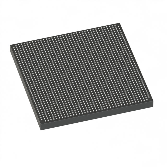
Stratix® V GX Field Programmable Gate Array (FPGA) IC 696 51200000 622000 1517-BBGA, FCBGA |
|---|---|
| Quantity | 948 Available (as of October 7, 2026) |
| Product Category | Field Programmable Gate Array (FPGA) |
|---|---|
| Manufacturer | Intel |
| Manufacturing Status | Active |
| Manufacturer Standard Lead Time | 26 Weeks |
| Datasheet |
Specifications & Environmental
| Device Package | 1517-FBGA (40x40) | Grade | Commercial | Operating Temperature | 0°C – 85°C | ||
|---|---|---|---|---|---|---|---|
| Package / Case | 1517-BBGA, FCBGA | Number of I/O | 696 | Voltage | 870 mV - 930 mV | ||
| Mounting Method | Surface Mount | RoHS Compliance | RoHS Compliant | REACH Compliance | REACH Unaffected | ||
| Moisture Sensitivity Level | 3 (168 Hours) | Number of LABs/CLBs | 234720 | Number of Logic Elements/Cells | 622000 | ||
| Number of Gates | N/A | ECCN | N/A | HTS Code | N/A | ||
| Qualification | N/A | Total RAM Bits | 51200000 |
Overview of 5SGXMA7K1F40C1G – Stratix® V GX FPGA, 622,000 logic elements, approximately 51.2 Mbits RAM, 696 I/O, 1517-FBGA
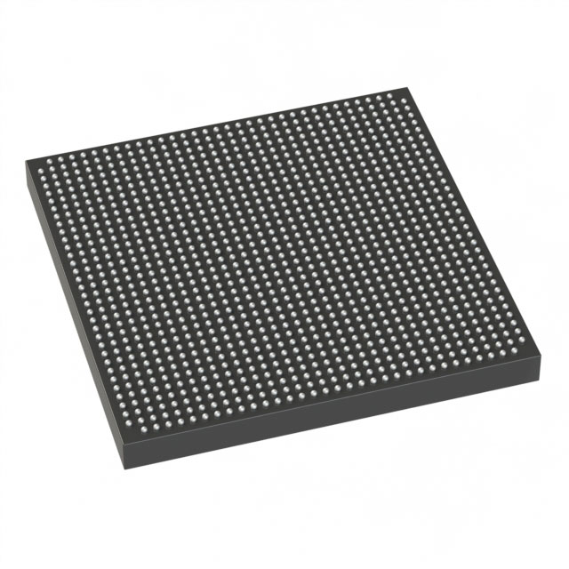
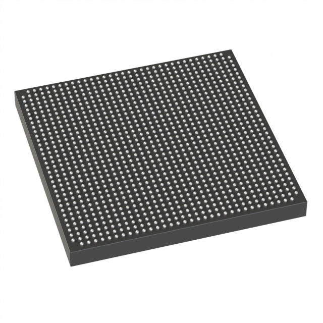
The 5SGXMA7K1F40C1G is a Stratix V GX Field Programmable Gate Array (FPGA) from Intel designed for high-density, high‑connectivity designs. It combines a large quantity of logic elements and on-chip memory with a high I/O count in a 1517‑FBGA surface‑mount package.
This device targets applications that require substantial programmable logic, significant embedded RAM capacity, and extensive board-level I/O while operating within commercial temperature limits. As a Stratix V GX device, the series data indicates support for multi‑Gbps transceiver speed grades.
Key Features
- Core Capacity 622,000 logic elements to implement large-scale digital logic and complex designs.
- Embedded Memory Approximately 51.2 Mbits of on-chip RAM for deep buffering, state storage, and data-intensive processing.
- I/O 696 user I/O pins to support wide parallel interfaces and dense board-level connectivity.
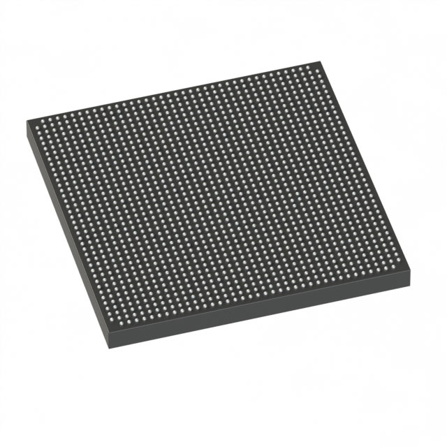
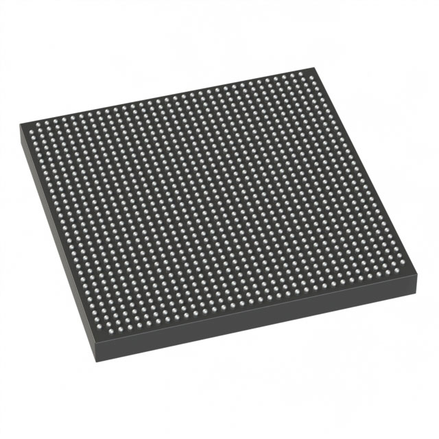
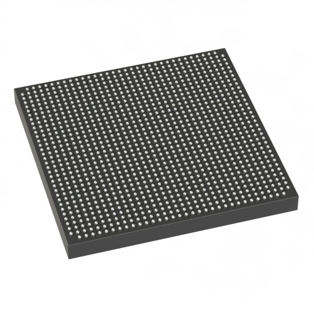
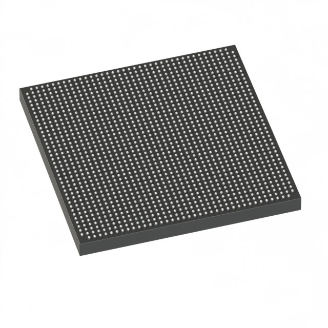
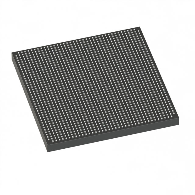
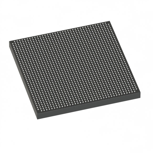
- Package & Mounting 1517‑BBGA / 1517‑FBGA (40×40) FCBGA, surface-mount for compact, high‑density PCB integration.
- Power Supply Core voltage supply range of 870 mV to 930 mV for core power budgeting and design planning.
- Operating Temperature Commercial grade operation from 0 °C to 85 °C.
- Stratix V GX Series Transceiver Capability Series documentation indicates support for GX transceiver speed grades (examples include 14.1 Gbps and 12.5 Gbps) for designs that require high-speed serial links.
- Compliance RoHS compliant.
Typical Applications
- High‑density digital processing Large logic capacity and abundant embedded RAM enable packet processing, protocol handling, and custom compute pipelines.
- High‑speed communications Stratix V GX series transceiver capability and numerous I/Os make the device suitable for telecom and networking line cards that require multi‑Gbps links.
- Data center and networking equipment Extensive I/O and on‑chip memory support switching, buffering, and data‑plane acceleration implementations.
- Complex board‑level integration High I/O count and a 1517‑FBGA package streamline integration into dense PCB designs requiring many external interfaces.
Unique Advantages
- High logic density: 622,000 logic elements provide the headroom to implement complex, multi‑module FPGA designs without partitioning across devices.
- Substantial on‑chip memory: Approximately 51.2 Mbits of embedded RAM reduces dependency on external RAM for buffering and stateful processing.
- Extensive connectivity: 696 I/O pins simplify routing of many parallel buses, interfaces, and external peripherals from a single device.
- Compact, board‑ready package: 1517‑FBGA (40×40) surface‑mount package supports high‑density PCB layouts and standard assembly flows.
- Commercial temperature and defined power: Commercial grade operation (0 °C to 85 °C) and a specified core voltage range (870–930 mV) aid thermal and power budgeting.
- Series transceiver options: Stratix V GX family documentation lists transceiver speed grades up to 14.1 Gbps for designs that need multi‑Gbps serial links.
Why Choose 5SGXMA7K1F40C1G?
The 5SGXMA7K1F40C1G places a very large logic fabric, substantial embedded memory, and a high I/O count into a single 1517‑FBGA package, making it well suited to engineers designing dense FPGA solutions that must consolidate functionality and minimize board count. Its commercial operating range and defined core voltage envelope make it straightforward to plan power and thermal solutions for production systems.
Designed as part of the Intel Stratix V GX family, this device is appropriate for projects that require high logic and memory capacity with series-level transceiver capability and extensive external interfacing. Use it where scalability, integration, and a documented device family datasheet are important selection criteria.
Request a quote or submit an RFQ to receive pricing, lead‑time, and availability information for the 5SGXMA7K1F40C1G.





















Date Founded: 1968
Headquarters: Santa Clara, California, USA
Employees: 130,000+
Revenue: $54.23 Billion
Certifications and Memberships: ISO9001:2015, ISO14001:2015, ISO17025:2017, ISO27001:2022, ISO45001:2018, ISO50001:2018


