
5SGXMA7K1F35I2N
| Part Description |
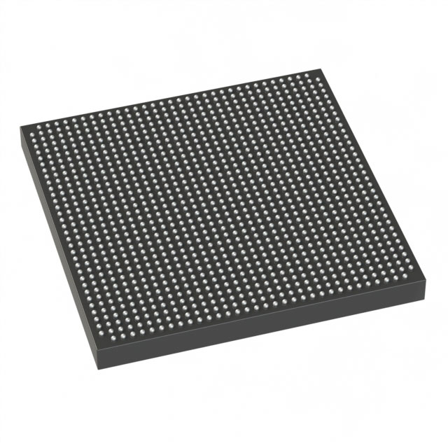
Stratix® V GX Field Programmable Gate Array (FPGA) IC 432 51200000 622000 1152-BBGA, FCBGA |
|---|---|
| Quantity | 565 Available (as of June 15, 2026) |

| Product Category | Field Programmable Gate Array (FPGA) |
|---|---|
| Manufacturer | Intel |
| Manufacturing Status | Obsolete |
| Manufacturer Standard Lead Time | Contact Us |
| Datasheet |
Specifications & Environmental
| Device Package | 1152-FBGA (35x35) | Grade | Industrial | Operating Temperature | -40°C – 100°C | ||
|---|---|---|---|---|---|---|---|
| Package / Case | 1152-BBGA, FCBGA | Number of I/O | 432 | Voltage | 870 mV - 930 mV | ||
| Mounting Method | Surface Mount | RoHS Compliance | RoHS Compliant | REACH Compliance | REACH Unknown | ||
| Moisture Sensitivity Level | 3 (168 Hours) | Number of LABs/CLBs | 234720 | Number of Logic Elements/Cells | 622000 | ||
| Number of Gates | N/A | ECCN | 3A001A2C | HTS Code | 8542.39.0001 | ||
| Qualification | N/A | Total RAM Bits | 51200000 |
Overview of 5SGXMA7K1F35I2N – Stratix® V GX Field Programmable Gate Array (FPGA) IC
The 5SGXMA7K1F35I2N is a high-density Stratix V GX Field Programmable Gate Array (FPGA) optimized for designs that require large logic capacity, significant on-chip memory, and extensive I/O. Built on the Stratix V GX family architecture, this device targets systems requiring programmable core logic combined with high-speed I/O and transceiver capabilities described for the Stratix V GX series.
With 622,000 logic elements, approximately 51.2 Mbits of embedded memory and 432 user I/O, this industrial-grade FPGA is suited for complex signal processing, high-throughput data movement, and dense integration in surface-mount BGA packages.
Key Features
- Core Logic 622,000 logic elements for large-scale programmable logic implementations and complex design partitioning.
- Embedded Memory Approximately 51.2 Mbits of total on-chip RAM to support buffering, FIFOs, and lookup-table storage for data-intensive processing.
- High-Density I/O 432 general-purpose I/O pins to support broad interfacing needs and dense board-level connectivity.
- Transceiver Family Capability Part of the Stratix V GX family, which includes transceiver speed grades documented up to 14.1 Gbps for GX channels in the series datasheet, enabling high-speed serial interfaces where required by the system design.
- Power and Voltage Core supply voltage range from 870 mV to 930 mV to match the device’s specified operating conditions.
- Package and Mounting Supplied in a 1152-BBGA FCBGA package (supplier package: 1152-FBGA, 35 × 35 mm) for compact, high-density PCB layouts; surface-mount mounting type.
- Industrial Temperature Grade Rated for operation from –40 °C to 100 °C, suitable for industrial-class environments.
- Compliance RoHS compliant for environmental and materials considerations.
Typical Applications
- High-speed serial communications Use the Stratix V GX family transceiver capabilities and abundant I/O for multi‑lane, high-throughput links and protocol bridging.
- Signal processing and compute acceleration Leverage 622,000 logic elements and ~51.2 Mbits of embedded RAM for real-time algorithms, filtering, and hardware-accelerated processing.
- Network and data center systems Combine high logic density and extensive I/O to implement packet processing, traffic management, and custom forwarding engines.
- Industrial control and automation Industrial temperature rating and flexible I/O make this FPGA suitable for robust control systems, motor control interfaces, and machine automation logic.
Unique Advantages
- High logic density: 622,000 logic elements enable integration of complex functions and reduces the need for multiple devices.
- Substantial on-chip memory: Approximately 51.2 Mbits of embedded RAM supports deep buffering and local data storage to improve throughput and latency.
- Extensive I/O count: 432 I/O pins provide flexibility for wide parallel buses, multiple interfaces, and board-level consolidation.
- Industrial temperature range: Rated –40 °C to 100 °C for designs that require reliable operation across extended ambient conditions.
- Compact BGA packaging: 1152-ball FCBGA (35 × 35 mm) supports high-density board designs while maintaining surface-mount compatibility.
- Standards-aligned supply requirements: Core voltage range of 870 mV to 930 mV aligns with the device’s specified electrical operating conditions.
Why Choose 5SGXMA7K1F35I2N?
The 5SGXMA7K1F35I2N offers a balance of high logic capacity, abundant embedded memory, and extensive I/O in an industrial-temperature FPGA package. It is positioned for system designs that need programmable hardware resources combined with the I/O and transceiver capabilities available in the Stratix V GX family.
Designers and procurement teams seeking a scalable platform for data-intensive, high-throughput, and industrial applications will find this device provides the integration and electrical characteristics necessary to simplify board-level design while supporting demanding workloads.
Request a quote or submit a request for additional purchasing information to evaluate the 5SGXMA7K1F35I2N for your next project.


Date Founded: 1968
Headquarters: Santa Clara, California, USA
Employees: 130,000+
Revenue: $54.23 Billion
Certifications and Memberships: ISO9001:2015, ISO14001:2015, ISO17025:2017, ISO27001:2022, ISO45001:2018, ISO50001:2018


