
A3P125-2FG144
| Part Description |
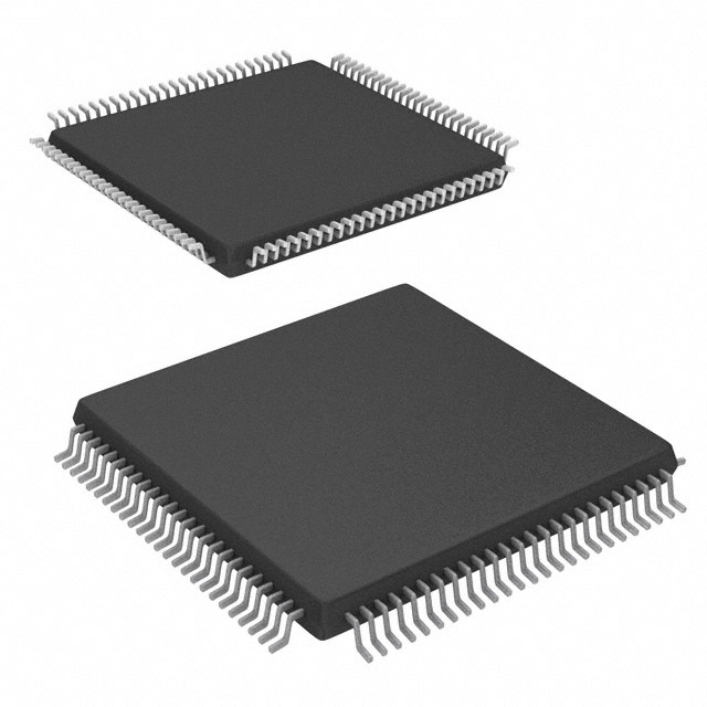
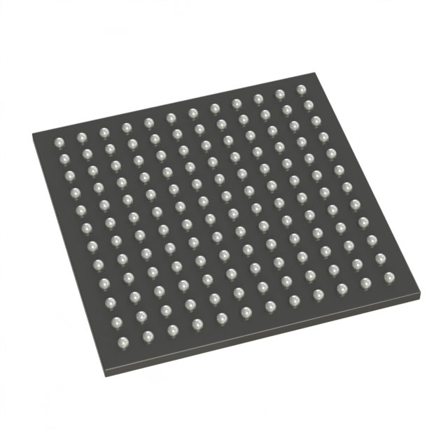
ProASIC3 Field Programmable Gate Array (FPGA) IC 97 36864 144-LBGA |
|---|---|
| Quantity | 270 Available (as of June 10, 2026) |

| Product Category | Field Programmable Gate Array (FPGA) |
|---|---|
| Manufacturer | Microchip Technology |
| Manufacturing Status | Active |
| Manufacturer Standard Lead Time | 10 Weeks |
| Datasheet |
Specifications & Environmental
| Device Package | 144-FPBGA (13x13) | Grade | Commercial | Operating Temperature | 0°C – 85°C | ||
|---|---|---|---|---|---|---|---|
| Package / Case | 144-LBGA | Number of I/O | 97 | Voltage | 1.425 V - 1.575 V | ||
| Mounting Method | Surface Mount | RoHS Compliance | RoHS non-compliant | REACH Compliance | REACH Unaffected | ||
| Moisture Sensitivity Level | 3 (168 Hours) | Number of LABs/CLBs | 3072 | Number of Logic Elements/Cells | 3072 | ||
| Number of Gates | 125000 | ECCN | 3A991D | HTS Code | 8542.39.0001 | ||
| Qualification | N/A | Total RAM Bits | 36864 |
Overview of A3P125-2FG144 – ProASIC3 Field Programmable Gate Array (FPGA) IC
The A3P125-2FG144 is a Microchip Technology ProASIC3 flash-based FPGA offered in a 144-LBGA package. It provides 3,072 logic elements, 36,864 bits of embedded RAM, and 97 user I/Os for implementing custom digital logic in commercial electronic designs.
Designed for surface-mount board assembly and operation across a commercial temperature range (0 °C to 85 °C), this device targets applications that require mid-density programmable logic with on-chip memory and flexible I/O in a compact 13 × 13 mm package footprint.
Key Features
- Core Logic 3,072 logic elements (cells) enabling implementation of custom combinational and sequential logic functions for mid-density designs.
- Embedded Memory 36,864 bits of on-chip RAM to store lookup tables, small buffers, and state information directly within the FPGA fabric.
- I/O 97 user I/O pins to support a range of peripheral interfaces and board-level connectivity.
- Gate Capacity Approximately 125,000 gates of equivalent logic capacity for mapping legacy gate-count requirements to programmable logic.
- Power Core supply range of 1.425 V to 1.575 V to match system power rails and enable predictable power budgeting.
- Package & Mounting 144-LBGA (Supplier package: 144-FPBGA 13×13) in a surface-mount form factor for compact PCB integration.
- Operating Range Commercial temperature grade with specified operation from 0 °C to 85 °C.
- Compliance RoHS-compliant device for designs requiring lead-free, environmentally conscious components.
Typical Applications
- Embedded Control Use the FPGA to implement application-specific control logic and finite-state machines where moderate logic density and on-chip RAM are required.
- Interface Bridging Deploy as a protocol or bus bridge using available I/O and logic elements to translate between digital interfaces on a board.
- Prototyping and Custom Logic Ideal for developing and validating custom logic functions and glue logic in commercial product development.
Unique Advantages
- Balanced Logic and Memory: 3,072 logic elements paired with 36,864 bits of RAM provide a balanced resource set for mid-density implementations without external memory.
- Significant I/O Count: 97 user I/Os support multiple peripheral connections, reducing the need for external interface chips.
- Compact, Surface-Mount Package: 144-LBGA (13×13) delivers a small PCB footprint for space-constrained designs.
- Predictable Power Range: Defined core voltage window (1.425 V–1.575 V) simplifies power-supply planning and integration.
- Commercial Temperature Suitability: Rated for 0 °C to 85 °C operation for standard commercial product deployments.
- RoHS Compliance: Supports environmentally regulated product designs and supply chain requirements.
Why Choose A3P125-2FG144?
The A3P125-2FG144 positions itself as a practical mid-density, flash-based FPGA for commercial designs that need a combination of logic elements, embedded RAM, and a substantial I/O complement in a compact LBGA package. Its defined supply voltage range and RoHS compliance make it straightforward to integrate into standard production environments.
This part is well suited to engineers and procurement teams seeking a Microchip Technology FPGA option for embedded control, interface bridging, and custom logic implementations where moderate gate count and on-chip memory are sufficient. The package and electrical specifications support streamlined PCB integration and predictable system behavior.
Request a quote or contact sales to discuss availability, pricing, and lead times for the A3P125-2FG144.


Date Founded: 1989
Headquarters: Chandler, Arizona, USA
Employees: 22,000+
Revenue: $8.349 Billion
Certifications and Memberships: ISO9001:2015, IATF16949:2016, AS 9100D


