
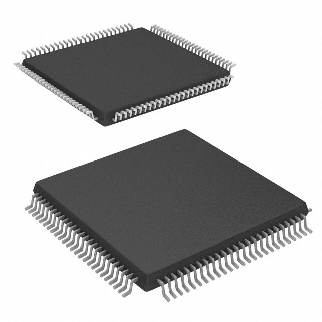
A3P250-1VQ100M
| Part Description |
ProASIC3 Field Programmable Gate Array (FPGA) IC 68 36864 100-TQFP |
|---|---|
| Quantity | 875 Available (as of June 15, 2026) |

| Product Category | Field Programmable Gate Array (FPGA) |
|---|---|
| Manufacturer | Microchip Technology |
| Manufacturing Status | Active |
| Manufacturer Standard Lead Time | 20 Weeks |
| Datasheet |
Specifications & Environmental
| Device Package | 100-VQFP (14x14) | Grade | Military | Operating Temperature | -55°C – 125°C | ||
|---|---|---|---|---|---|---|---|
| Package / Case | 100-TQFP | Number of I/O | 68 | Voltage | 1.425 V - 1.575 V | ||
| Mounting Method | Surface Mount | RoHS Compliance | RoHS non-compliant | REACH Compliance | REACH Unaffected | ||
| Moisture Sensitivity Level | 3 (168 Hours) | Number of LABs/CLBs | 6144 | Number of Logic Elements/Cells | 6144 | ||
| Number of Gates | 250000 | ECCN | 3A001A2C | HTS Code | 8542.39.0001 | ||
| Qualification | MIL-STD-883 | Total RAM Bits | 36864 |
Overview of A3P250-1VQ100M – ProASIC3 Field Programmable Gate Array (FPGA) IC 68 36864 100-TQFP
The A3P250-1VQ100M is a ProASIC3 field programmable gate array (FPGA) IC from Microchip Technology designed for military-grade applications. It combines mid-range logic capacity with on-chip memory and a broad I/O complement in a 100-pin TQFP package, offering a compact, qualified programmable logic option for designs that require proven environmental and qualification characteristics.
This device is specified for military qualification to MIL-STD-883 and rated for operation from -55 °C to 125 °C, making it suitable for mission-critical and rugged embedded systems that demand traceable qualification and wide-temperature operation.
Key Features
- Logic Capacity Approximately 6,144 logic elements delivering around 250,000 equivalent gates for mid-range programmable logic implementations.
- Embedded Memory Total on-chip RAM of 36,864 bits, approximately 0.037 Mbits of embedded memory for small buffers, state storage, and control logic.
- I/O Count 68 user I/O pins to support multiple interfaces, peripheral connections, and board-level signal routing.
- Power Supply Specified core voltage range of 1.425 V to 1.575 V to match targeted system power domains.
- Package and Mounting 100-TQFP package (supplier device package: 100-VQFP, 14 × 14 mm) with surface-mount construction for compact PCB implementations.
- Qualification and Grade Military grade with MIL-STD-883 qualification, supporting designs that require established military test standards.
- Operating Temperature Wide operating temperature range from -55 °C to 125 °C suitable for harsh environmental deployments.
- Environmental Compliance RoHS compliant.
Typical Applications
- Defense and Military Electronics Programmable logic for mission-critical control, interface bridging, and custom processing where MIL-STD-883 qualification and wide temperature operation are required.
- Aerospace Systems Control logic, sensor interfacing, and custom glue logic in avionics and airborne equipment operating across extended temperature ranges.
- Ruggedized Embedded Control Industrial and field-deployed systems that need robust, qualified programmable logic in a compact surface-mount package.
Unique Advantages
- Military-Qualified Reliability: MIL-STD-883 qualification and a -55 °C to 125 °C operating range support usage in harsh and mission-critical environments.
- Compact, Integrated Logic: Approximately 6,144 logic elements and 250,000 gates provide a balance of density and integration for mid-range FPGA tasks, reducing the need for multiple discrete components.
- On-Board Memory: Approximately 0.037 Mbits of embedded RAM for control states, small FIFOs, and buffering without external memory.
- Flexible I/O Count: 68 I/O pins enable multiple peripheral and interface connections from a single device footprint.
- Surface-Mount 100-TQFP Package: Standard 100-pin TQFP (14 × 14 mm) package supports compact PCB layouts and established assembly processes.
- Regulatory and Environmental Compliance: RoHS compliance supports modern environmental requirements for electronic assemblies.
Why Choose A3P250-1VQ100M?
The A3P250-1VQ100M positions itself as a military-grade FPGA option that balances logic capacity, I/O flexibility, and on-chip memory in a compact 100-pin TQFP package. Its MIL-STD-883 qualification and wide operating temperature range make it appropriate for designers building rugged, mission-critical systems that require traceable qualification and dependable electrical characteristics.
Backed by Microchip Technology, this FPGA is suited for engineers and procurement teams seeking a mid-range programmable logic device for defense, aerospace, and other harsh-environment embedded applications where proven qualification and compact integration are priorities.
Request a quote or submit an inquiry to get pricing and availability for the A3P250-1VQ100M.


Date Founded: 1989
Headquarters: Chandler, Arizona, USA
Employees: 22,000+
Revenue: $8.349 Billion
Certifications and Memberships: ISO9001:2015, IATF16949:2016, AS 9100D


