
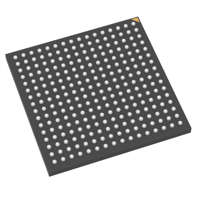
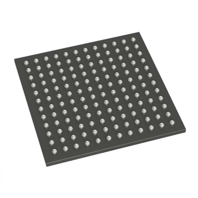
A3P250-2FG144
| Part Description |
ProASIC3 Field Programmable Gate Array (FPGA) IC 97 36864 144-LBGA |
|---|---|
| Quantity | 1,495 Available (as of June 15, 2026) |

| Product Category | Field Programmable Gate Array (FPGA) |
|---|---|
| Manufacturer | Microchip Technology |
| Manufacturing Status | Active |
| Manufacturer Standard Lead Time | 10 Weeks |
| Datasheet |
Specifications & Environmental
| Device Package | 144-FPBGA (13x13) | Grade | Commercial | Operating Temperature | 0°C – 85°C | ||
|---|---|---|---|---|---|---|---|
| Package / Case | 144-LBGA | Number of I/O | 97 | Voltage | 1.425 V - 1.575 V | ||
| Mounting Method | Surface Mount | RoHS Compliance | RoHS non-compliant | REACH Compliance | REACH Unaffected | ||
| Moisture Sensitivity Level | 3 (168 Hours) | Number of LABs/CLBs | 6144 | Number of Logic Elements/Cells | 6144 | ||
| Number of Gates | 250000 | ECCN | 3A991D | HTS Code | 8542.39.0001 | ||
| Qualification | N/A | Total RAM Bits | 36864 |
Overview of A3P250-2FG144 – ProASIC3 FPGA, 97 I/O, 36,864-bit RAM, 144-LBGA
The A3P250-2FG144 is a ProASIC3 field programmable gate array (FPGA) IC designed for commercial embedded applications. It integrates 6,144 logic elements, approximately 36.9 kbits of on-chip RAM and 97 I/O in a compact 144-LBGA package to deliver a balanced combination of logic capacity and I/O density.
This device targets designs that require configurable digital logic with defined supply and thermal ranges—featuring a core voltage range of 1.425 V to 1.575 V and an operating temperature range of 0 °C to 85 °C—while maintaining RoHS compliance and surface-mount mounting for modern PCB assembly.
Key Features
- Core Logic 6,144 logic elements (LAB/CLB equivalent) providing a usable logic fabric and an approximate gate count of 250,000 for implementing moderate-density designs.
- On‑Chip Memory Approximately 36.9 kbits (36,864 bits) of embedded RAM for small buffers, FIFOs and state storage directly inside the device.
- I/O Density 97 user I/O pins to support a wide range of peripheral interfaces and board-level interconnect requirements.
- Supply and Thermal Defined core voltage range of 1.425 V to 1.575 V and an operating temperature range of 0 °C to 85 °C suitable for commercial applications.
- Package & Mounting 144-LBGA package (supplier device package: 144-FPBGA, 13×13) with surface-mount mounting for space-efficient PCB integration.
- Regulatory RoHS compliant, supporting modern environmental and manufacturing requirements.
- Grade Commercial grade component intended for general-purpose embedded systems and commercial products.
Typical Applications
- Commercial embedded systems Use where a compact FPGA with 6,144 logic elements and 97 I/O supports peripheral control, glue logic or protocol bridging within a commercial product.
- Board-level I/O expansion Deploy as a dedicated logic device to add customizable I/O handling and signal aggregation on space-constrained PCBs using the 144-LBGA package.
- Prototyping and evaluation Suitable for evaluating moderate-density FPGA implementations that require on-chip memory and a clearly defined supply and temperature envelope.
Unique Advantages
- Balanced logic-to-I/O ratio: 6144 logic elements paired with 97 I/O pins enables efficient mapping of medium-complexity logic functions without oversizing the device.
- Compact LBGA footprint: The 144-LBGA (13×13) package helps minimize board area while providing adequate I/O count for many commercial designs.
- Defined electrical operating window: A narrow core voltage range (1.425 V–1.575 V) simplifies power-supply planning and helps ensure consistent device behavior within specified limits.
- On-chip RAM for local buffering: Approximately 36.9 kbits of embedded memory reduces external memory needs for small FIFO/buffer tasks and state storage.
- RoHS compliant and surface mount: Meets common environmental standards and is compatible with standard surface-mount assembly processes.
Why Choose A3P250-2FG144?
The A3P250-2FG144 offers a practical balance of logic resources, embedded memory and I/O in a compact commercial-grade LBGA package. Its specification set—6,144 logic elements, roughly 36.9 kbits of on-chip RAM, 97 I/O, and a clear supply/temperature window—makes it well suited for designers who need a configurable logic device for commercial embedded applications with controlled power and thermal requirements.
For teams seeking a straightforward FPGA integration with RoHS compliance and surface-mount packaging, the A3P250-2FG144 provides predictable electrical and mechanical characteristics that simplify board-level design and procurement.
Request a quote or submit a purchasing inquiry to obtain pricing and lead-time information for the A3P250-2FG144. Our team can provide availability and help with order placement.


Date Founded: 1989
Headquarters: Chandler, Arizona, USA
Employees: 22,000+
Revenue: $8.349 Billion
Certifications and Memberships: ISO9001:2015, IATF16949:2016, AS 9100D


