
A3P250-2FG256
| Part Description |
ProASIC3 Field Programmable Gate Array (FPGA) IC 157 36864 256-LBGA |
|---|---|
| Quantity | 976 Available (as of June 10, 2026) |

| Product Category | Field Programmable Gate Array (FPGA) |
|---|---|
| Manufacturer | Microchip Technology |
| Manufacturing Status | Active |
| Manufacturer Standard Lead Time | 10 Weeks |
| Datasheet |
Specifications & Environmental
| Device Package | 256-FPBGA (17x17) | Grade | Commercial | Operating Temperature | 0°C – 85°C | ||
|---|---|---|---|---|---|---|---|
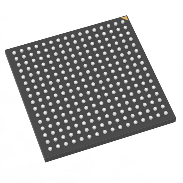
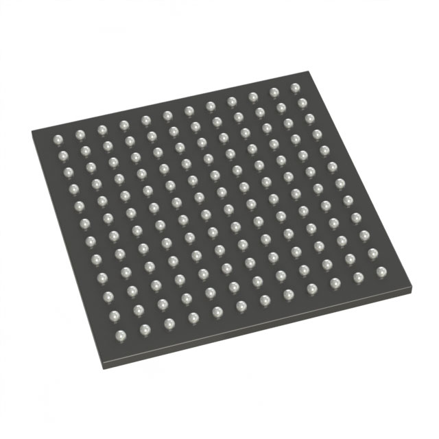
| Package / Case | 256-LBGA | Number of I/O | 157 | Voltage | 1.425 V - 1.575 V | ||
| Mounting Method | Surface Mount | RoHS Compliance | RoHS non-compliant | REACH Compliance | REACH Unaffected | ||
| Moisture Sensitivity Level | 3 (168 Hours) | Number of LABs/CLBs | 6144 | Number of Logic Elements/Cells | 6144 | ||
| Number of Gates | 250000 | ECCN | 3A991D | HTS Code | 8542.39.0001 | ||
| Qualification | N/A | Total RAM Bits | 36864 |
Overview of A3P250-2FG256 – ProASIC3 Field Programmable Gate Array (FPGA) IC 157 36864 256-LBGA
The A3P250-2FG256 is a ProASIC3 field programmable gate array (FPGA) supplied in a 256-LBGA package. It integrates programmable logic, on-chip memory and a high I/O count to support custom digital functions and interface logic for commercial embedded systems.
With 6,144 logic elements, approximately 0.037 Mbits of embedded memory and 157 I/O pins, this device targets designs that require moderate logic capacity, dense external connectivity and a compact surface-mount package.
Key Features
- Core Logic 6,144 logic elements provide programmable resources for implementing custom digital functions and state machines.
- Embedded Memory Approximately 0.037 Mbits (36,864 bits) of on-chip RAM for small buffers, FIFOs and distributed storage.
- I/O Density 157 user I/O pins to support multiple interfaces and parallel connections to external devices.
- Gate Count 250,000 gates for mapping combinational and sequential logic in mid-range designs.
- Power Supply Operates from a supply range of 1.425 V to 1.575 V to match target system power rails.
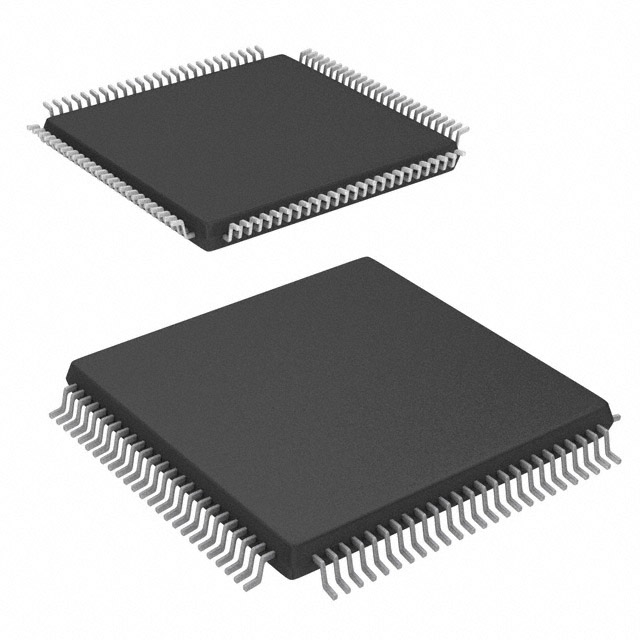
- Package & Mounting 256-LBGA surface-mount package (supplier device package: 256-FPBGA 17×17) for compact PCB implementations.
- Temperature & Grade Commercial grade device rated for 0°C to 85°C operating temperature range.
- RoHS Compliance RoHS compliant to meet common environmental and manufacturing requirements.
Typical Applications
- Interface and Glue Logic Use the device’s 157 I/Os and logic elements to implement protocol bridging, bus interfacing and signal conditioning between system components.
- Embedded Control Implement control finite-state machines, timing logic and peripheral management within compact embedded products.
- Prototyping and Functional Verification Suitable for evaluating mid-range programmable designs where moderate logic capacity and on-chip RAM are required.
- Sensor and I/O Aggregation Aggregate multiple sensor inputs or peripheral signals using the device’s I/O count and programmable logic to simplify upstream processing.
Unique Advantages
- Balanced Logic and Memory 6,144 logic elements paired with 36,864 bits of embedded RAM provide a practical balance for control logic plus local buffering without external memory.
- High I/O Count in a Compact Footprint 157 I/Os in a 256-LBGA package enable dense board-level integration while preserving I/O flexibility.
- Compact Surface-Mount Package The 256-FPBGA (17×17) package supports compact PCB layouts and automated assembly processes.
- Commercial Temperature Range Rated 0°C to 85°C for a wide range of standard commercial applications.
- Regulatory Compliance RoHS compliance supports common environmental manufacturing requirements.
Why Choose A3P250-2FG256?
The A3P250-2FG256 delivers a practical combination of programmable logic, on-chip memory and a high I/O complement in a compact 256-LBGA surface-mount package. Its specifications make it well suited for mid-range embedded designs that require custom digital logic, multiple external interfaces and modest local memory.
Designers and procurement teams seeking a commercially graded FPGA with clear supply-voltage and temperature specifications will find this device appropriate for applications where board space, I/O density and verified programmable resources matter. Its resource mix supports scalable implementations and straightforward integration into existing platforms.
Request a quote or submit an inquiry to obtain pricing, lead time and ordering information for the A3P250-2FG256.


Date Founded: 1989
Headquarters: Chandler, Arizona, USA
Employees: 22,000+
Revenue: $8.349 Billion
Certifications and Memberships: ISO9001:2015, IATF16949:2016, AS 9100D


