
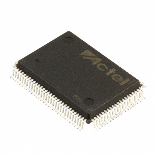
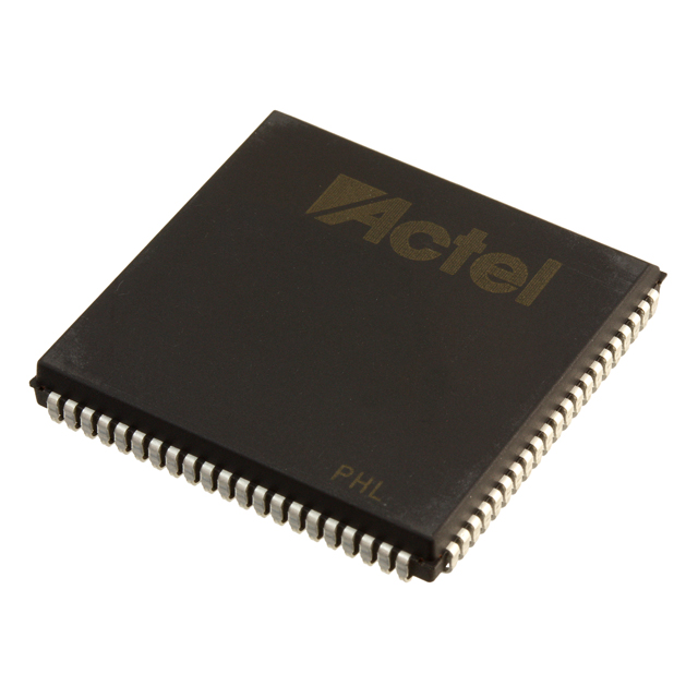
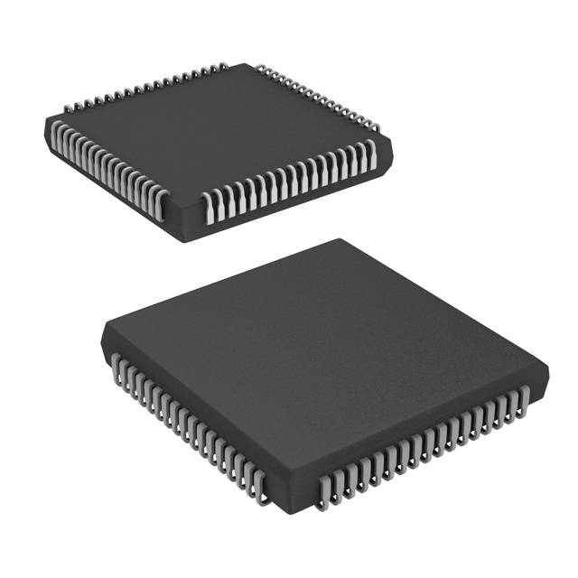
A40MX04-3PLG68
| Part Description |
MX Field Programmable Gate Array (FPGA) IC 57 68-LCC (J-Lead) |
|---|---|
| Quantity | 1,211 Available (as of June 10, 2026) |

| Product Category | Field Programmable Gate Array (FPGA) |
|---|---|
| Manufacturer | Microchip Technology |
| Manufacturing Status | Active |
| Manufacturer Standard Lead Time | 12 Weeks |
| Datasheet |
Specifications & Environmental
| Device Package | 68-PLCC (24.23x24.23) | Grade | Commercial | Operating Temperature | 0°C – 70°C | ||
|---|---|---|---|---|---|---|---|
| Package / Case | 68-LCC (J-Lead) | Number of I/O | 57 | Voltage | 3 V - 5.25 V | ||
| Mounting Method | Surface Mount | RoHS Compliance | ROHS3 Compliant | REACH Compliance | REACH Unaffected | ||
| Moisture Sensitivity Level | 3 (168 Hours) | Number of LABs/CLBs | 547 | Number of Logic Elements/Cells | 547 | ||
| Number of Gates | 6000 | ECCN | 3A991D | HTS Code | 8542.39.0001 | ||
| Qualification | N/A |
Overview of A40MX04-3PLG68 – MX Field Programmable Gate Array (FPGA) IC, 57 I/O, 68-LCC (J-Lead)
The A40MX04-3PLG68 is a field programmable gate array (FPGA) in a 68‑lead LCC (J‑lead) surface‑mount package designed for commercial applications. It provides moderate-density programmable logic with 547 logic elements (LEs) and 57 general‑purpose I/O pins, supporting designs that require configurable glue logic, custom interfaces, or small control/state machines.
Key hardware attributes include a 3.0 V to 5.25 V supply range, commercial operating temperature from 0 °C to 70 °C, and RoHS compliance, making it suitable for a broad set of commercial embedded designs that need board‑level integration in a compact PLCC footprint.
Key Features
- Logic Capacity 547 logic elements (LEs) delivering approximately 6,000 gates worth of programmable logic for mid‑density designs.
- I/O Resources 57 general‑purpose I/O pins to support multiple peripheral interfaces and custom signal routing on a single device.
- Memory No embedded RAM bits; suitable for designs that use external memory or are focused on combinational and small sequential logic functions.
- Voltage Flexibility Operates from 3.0 V to 5.25 V, enabling compatibility with common commercial logic rails and mixed‑voltage designs within that range.
- Package & Mounting 68‑lead LCC (J‑lead) package in a 24.23 × 24.23 mm footprint, optimized for surface‑mount assembly on standard PCBs.
- Commercial Grade Rated for 0 °C to 70 °C operation and designated as commercial grade for general‑purpose applications.
- Environmental Compliance RoHS compliant to support environmentally conscious product designs.
Typical Applications
- Commercial Embedded Control Implement compact control logic and state machines for consumer and commercial equipment operating within commercial temperature ranges.
- Interface Bridging & Glue Logic Provide protocol translation, bus bridging, and custom signal conditioning between disparate subsystems using available I/O and programmable logic.
- Prototyping & Development Evaluate mid‑density FPGA architectures or prototype custom logic functions before committing to larger FPGA or ASIC solutions.
- User‑Defined Peripheral Control Drive bespoke peripheral timing, I/O aggregation, and simple sequencers in compact PCB form factors.
Unique Advantages
- Moderate Logic Density: 547 logic elements (approximately 6,000 gates) provide a balance between capability and cost for mid‑range programmable tasks.
- Substantial I/O Count: 57 I/O pins enable multiple interface implementations and flexible board integration without immediate need for I/O expanders.
- Wide Supply Voltage Range: 3.0 V to 5.25 V operation allows integration with common commercial voltage domains.
- Standard PLCC Footprint: 68‑lead LCC (J‑lead) package simplifies replacement or retrofit into existing PLCC‑based designs and supports surface‑mount assembly.
- Commercial Temperature Rating: Rated for 0 °C to 70 °C operation to match typical commercial product environments.
- RoHS Compliant: Meets RoHS environmental requirements for regulated markets and supply chains.
Why Choose A40MX04-3PLG68?
The A40MX04-3PLG68 positions itself as a practical mid‑density FPGA option for commercial designs that need flexible programmable logic, a healthy complement of I/O, and compatibility with standard PCB assembly processes. Its 547 logic elements and 57 I/O pins make it well suited for glue logic, interface adaptation, and control‑oriented tasks where on‑chip RAM is not required.
For development teams and product engineers seeking a commercially rated, RoHS‑compliant FPGA in a compact 68‑lead LCC package, the A40MX04-3PLG68 provides a straightforward, board‑level programmable solution with supply voltage flexibility and surface‑mount mounting for efficient integration.
Request a quote or submit a pricing inquiry to receive availability and lead‑time information for the A40MX04-3PLG68.


Date Founded: 1989
Headquarters: Chandler, Arizona, USA
Employees: 22,000+
Revenue: $8.349 Billion
Certifications and Memberships: ISO9001:2015, IATF16949:2016, AS 9100D


