
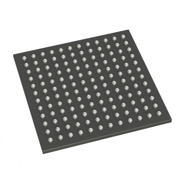
A54SX08-1FG144
| Part Description |
SX Field Programmable Gate Array (FPGA) IC 111 144-LBGA |
|---|---|
| Quantity | 827 Available (as of June 15, 2026) |

| Product Category | Field Programmable Gate Array (FPGA) |
|---|---|
| Manufacturer | Microchip Technology |
| Manufacturing Status | Active |
| Manufacturer Standard Lead Time | 52 Weeks |
| Datasheet |
Specifications & Environmental
| Device Package | 144-FPBGA (13x13) | Grade | Commercial | Operating Temperature | 0°C – 70°C | ||
|---|---|---|---|---|---|---|---|
| Package / Case | 144-LBGA | Number of I/O | 111 | Voltage | 3 V - 5.25 V | ||
| Mounting Method | Surface Mount | RoHS Compliance | RoHS non-compliant | REACH Compliance | REACH Unaffected | ||
| Moisture Sensitivity Level | 3 (168 Hours) | Number of LABs/CLBs | 768 | Number of Logic Elements/Cells | 768 | ||
| Number of Gates | 12000 | ECCN | 3A991D | HTS Code | 8542.39.0001 | ||
| Qualification | N/A |
Overview of A54SX08-1FG144 – SX Field Programmable Gate Array (FPGA) IC 111 144-LBGA
The A54SX08-1FG144 is an SX-A family Field Programmable Gate Array from Microchip Technology supplied in a 144-ball fine-pitch BGA / 144-LBGA surface-mount package. It provides a nonvolatile, single-chip FPGA solution with approximately 12,000 system gates and 768 logic elements, and is targeted at designs that require reconfigurable logic, mixed-voltage I/O support and in-system diagnostic capability.
Designed for commercial-temperature applications (0 °C to 70 °C), the device supports mixed 2.5 V, 3.3 V and 5 V I/O schemes and a supply range of 3 V to 5.25 V, enabling flexible interfacing in a variety of embedded and PCI-capable systems.
Key Features
- Core capacity — Approximately 12,000 system gates and 768 logic elements provide on-chip programmable logic for glue logic, protocol bridging and control functions.
- Performance — SX-A family characteristics include up to 250 MHz system performance and up to 350 MHz internal performance; the –1 speed grade is approximately 15% faster than standard.
- I/O flexibility — 111 user I/Os with configurable support for 3.3 V / 5 V PCI, 5 V TTL, 3.3 V LVTTL and 2.5 V LVCMOS2; 5 V input tolerance and 5 V drive strength enable mixed-voltage designs and direct interfacing to a wide range of peripherals.
- Nonvolatile single-chip solution — Device stores configuration on-chip, eliminating the need for external configuration memory and simplifying board design.
- System and test features — Boundary-scan testing compliant with IEEE 1149.1 (JTAG) and unique in-system diagnostic and verification capability using Silicon Explorer II (family feature).
- Security — Actel Secure Programming Technology with FuseLock™ to protect design IP from reverse engineering (family feature).
- Package and mounting — 144-ball fine-pitch BGA / 144-LBGA surface-mount package (supplier device package: 144-FPBGA 13×13), compact footprint for space-constrained boards.
- Power and environmental — Operating supply range 3 V to 5.25 V; commercial temperature grade 0 °C to 70 °C; RoHS compliant.
Typical Applications
- PCI and peripheral interfaces — Use the device’s PCI-compliant I/O and 66 MHz PCI support to implement interface logic and protocol handling for add-on cards and peripheral modules.
- Mixed-voltage system glue logic — Flexible I/O voltage support and 5 V tolerance make the FPGA suitable for bridging between logic domains and integrating legacy 5 V signals with modern 3.3 V or 2.5 V subsystems.
- Embedded control and custom logic — With ~12,000 system gates and 768 logic elements, implement control state machines, custom datapaths and peripheral controllers in a single-chip solution.
- In-system verification and diagnostics — Leverage the family’s Silicon Explorer II capability and JTAG boundary-scan for on-board verification and fault isolation during development and production testing.
Unique Advantages
- Highly integrated, nonvolatile FPGA: On-chip configuration removes the need for external configuration memory, reducing BOM and simplifying power-up sequencing.
- Flexible mixed-voltage I/O: Configurable I/O standards and 5 V tolerance allow direct interfacing to different logic families without level-shifters in many cases.
- Compact, production-ready package: 144-ball fine-pitch BGA / 144-LBGA in a surface-mount format saves board area while delivering 111 user I/Os.
- Deterministic timing and diagnostics: Family-level support for deterministic, user-controllable timing plus in-system diagnostic tools aids timing closure and debug.
- Security features: FuseLock programming technology helps protect intellectual property and prevent reverse engineering.
- RoHS-compliant commercial solution: Designed for commercial-temperature systems with RoHS-compliant packaging for regulatory compliance.
Why Choose A54SX08-1FG144?
The A54SX08-1FG144 combines a compact fine-pitch BGA package with a nonvolatile SX-A family FPGA architecture to deliver reprogrammable logic, flexible mixed-voltage I/O and built-in diagnostic and security features. With approximately 12,000 system gates, 768 logic elements and 111 user I/Os, it is a practical choice for designers implementing interface logic, protocol bridges, and embedded control functions in commercial-temperature products.
Its on-chip configuration, configurable I/O standards, and family-level tools for in-system verification provide a streamlined integration path that reduces external components, eases board-level testing, and helps protect design IP.
Request a quote or contact sales to check availability and pricing for the A54SX08-1FG144.


Date Founded: 1989
Headquarters: Chandler, Arizona, USA
Employees: 22,000+
Revenue: $8.349 Billion
Certifications and Memberships: ISO9001:2015, IATF16949:2016, AS 9100D


