
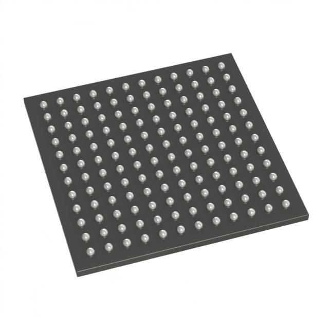
A54SX08-2FG144
| Part Description |
SX Field Programmable Gate Array (FPGA) IC 111 144-LBGA |
|---|---|
| Quantity | 680 Available (as of June 15, 2026) |

| Product Category | Field Programmable Gate Array (FPGA) |
|---|---|
| Manufacturer | Microchip Technology |
| Manufacturing Status | Active |
| Manufacturer Standard Lead Time | 52 Weeks |
| Datasheet |
Specifications & Environmental
| Device Package | 144-FPBGA (13x13) | Grade | Commercial | Operating Temperature | 0°C – 70°C | ||
|---|---|---|---|---|---|---|---|
| Package / Case | 144-LBGA | Number of I/O | 111 | Voltage | 3 V - 5.25 V | ||
| Mounting Method | Surface Mount | RoHS Compliance | RoHS non-compliant | REACH Compliance | REACH Unaffected | ||
| Moisture Sensitivity Level | 3 (168 Hours) | Number of LABs/CLBs | 768 | Number of Logic Elements/Cells | 768 | ||
| Number of Gates | 12000 | ECCN | 3A991D | HTS Code | 8542.39.0001 | ||
| Qualification | N/A |
Overview of A54SX08-2FG144 – SX Field Programmable Gate Array (FPGA) IC 111 144-LBGA
The A54SX08-2FG144 is a member of the SX-A family of nonvolatile, single-chip FPGAs designed for moderate-density programmable logic applications. This device provides 12,000 system gates implemented as 768 logic elements with up to 111 user I/Os in a compact 144-ball BGA package, making it suitable for designs that require mixed-voltage I/O and deterministic timing control.
Built for commercial-temperature operation, the device supports 3.0 V to 5.25 V supply ranges and offers family-level features such as hot-swap–capable I/Os, configurable I/O standards, and in-system diagnostic capabilities for verification and security.
Key Features
- Logic Capacity 768 logic elements (combinatorial cells) delivering approximately 12,000 system gates for moderate-density logic integration.
- User I/O Up to 111 user-programmable I/O pins with configurable pull-up/pull-down behavior at power-up and individual output slew rate control.
- Mixed-Voltage I/O and Tolerance Supports configurable I/O for 2.5 V, 3.3 V, and 5 V signaling with 5 V input tolerance and 5 V drive strength options as supported across the SX-A family.
- Performance Family-level performance indicators include up to 250 MHz system performance and up to 350 MHz internal performance (SX-A family specifications).
- Nonvolatile Single-Chip Architecture Single-chip, nonvolatile FPGA eliminates the need for external configuration memory.
- System and Board Compatibility Hot-swap–compliant I/Os and 66 MHz PCI compliance at the family level for interfacing with legacy PCI systems where required.
- Package and Mounting 144-LBGA package (supplier device package: 144-FPBGA 13×13) in a surface-mount form factor optimized for compact board layouts.
- Commercial Temperature Grade Rated for commercial operation from 0 °C to 70 °C.
- Security and Testability Family features include Actel FuseLock™ secure programming technology and IEEE 1149.1 (JTAG) boundary-scan testing support, plus in-system diagnostic and verification with Silicon Explorer II.
- Regulatory RoHS compliant.
Typical Applications
- Embedded Control Integrate glue logic, state machines, and control functions in compact embedded systems using 768 logic elements and up to 111 I/Os for sensor and actuator interfaces.
- Interface Bridging Implement mixed-voltage protocol translation and I/O conditioning where 2.5 V, 3.3 V and 5 V signaling and 5 V tolerance are required.
- Legacy PCI Subsystems Use the device in peripheral or bridge designs that require PCI signaling compatibility (66 MHz PCI compliance at the family level).
- In-System Diagnostics and Verification Deploy devices that benefit from built-in diagnostic and verification workflows using the Silicon Explorer II capability for field troubleshooting and validation.
Unique Advantages
- Nonvolatile, single-chip solution: Reduces BOM and board complexity by removing the need for external configuration memory.
- Mixed-voltage I/O flexibility: Configurable I/O standards and 5 V tolerance facilitate interfacing to a wide range of legacy and modern logic levels.
- Deterministic timing control: Family-level deterministic, user-controllable timing enables predictable performance for timing-sensitive designs.
- Compact, surface-mount package: 144-ball BGA (144-FPBGA 13×13) delivers a small footprint for space-constrained PCBs while providing extensive I/O.
- Integrated security and test features: FuseLock secure programming and IEEE 1149.1 boundary-scan support help protect IP and simplify board-level testing.
- Commercial-grade reliability: Designed for 0 °C to 70 °C operation with RoHS-compliant packaging for mainstream electronic products.
Why Choose A54SX08-2FG144?
The A54SX08-2FG144 combines a nonvolatile, single-chip FPGA architecture with moderate logic capacity and a broad, configurable I/O set to address compact embedded designs that need mixed-voltage interfacing and predictable timing. Its 144-ball BGA package and surface-mount mounting make it well suited for space-conscious board layouts while maintaining up to 111 user I/Os.
Engineers seeking a commercial-grade FPGA with family-proven features—such as hot-swap–capable I/Os, in-system diagnostics, boundary-scan testing, and secure programming—will find the A54SX08-2FG144 provides integration and testability advantages that simplify system design and deployment.
Request a quote or submit an inquiry for pricing and availability to evaluate the A54SX08-2FG144 for your next design.


Date Founded: 1989
Headquarters: Chandler, Arizona, USA
Employees: 22,000+
Revenue: $8.349 Billion
Certifications and Memberships: ISO9001:2015, IATF16949:2016, AS 9100D


